Analog and digital circuits are the two main building blocks used in the field of electronics. Continuous signals, such as voltages or currents that change over time, are handled by analog circuits. Conversely, discrete bits of information are processed by digital circuits.
This gap is filled by analog and mixed-signal (AMS) design. Its main goal is to build integrated circuits that smoothly blend digital and analog features. These integrated circuits (ICs) are the basis of contemporary electronics, enabling everything from ultra-precise sensors in smartphones to high-fidelity audio amplifiers. In today’s landscape, AMS design is mission-critical for AI data centers and 5G-Advanced infrastructure, where high-speed data translation is the primary bottleneck.
Hardware PCB layout and design expertise are crucial for translating AMS concepts into real-world, functional devices. This blog will delve deeper into the intricacies of AMS design, with a specific focus on the essential role of hardware design.
Current Landscape of AMS Design
The analog and mixed signal device market is continually evolving in response to the increasing demand for downsizing, enhanced performance, and reduced power consumption.
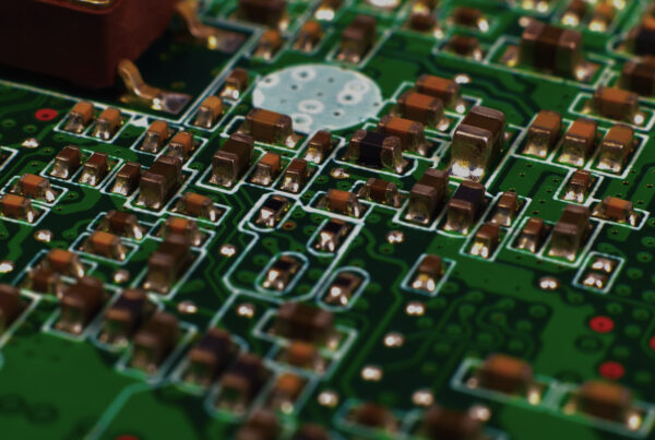
A dizzying array of analog, digital, and radio frequency (RF) components is integrated into modern integrated circuits. Engineers are increasingly utilizing Heterogeneous Integration, where components from different manufacturing nodes are combined into a single package to maximize both logic density and analog precision. Advanced design techniques and tools are required to control their interactions and guarantee smooth functioning.
The main obstacles that PCB hardware designers face are numerous. In high-density circuits, maintaining signal purity and controlling power integrity becomes harder to achieve. To overcome these obstacles, creativity must never stop. To increase performance, novel materials like Silicon Carbide (SiC) and Gallium Nitride (GaN) are being investigated. To get over space restrictions, more sophisticated design methods like 3D integration are being developed.
Future Trends in AMS Design
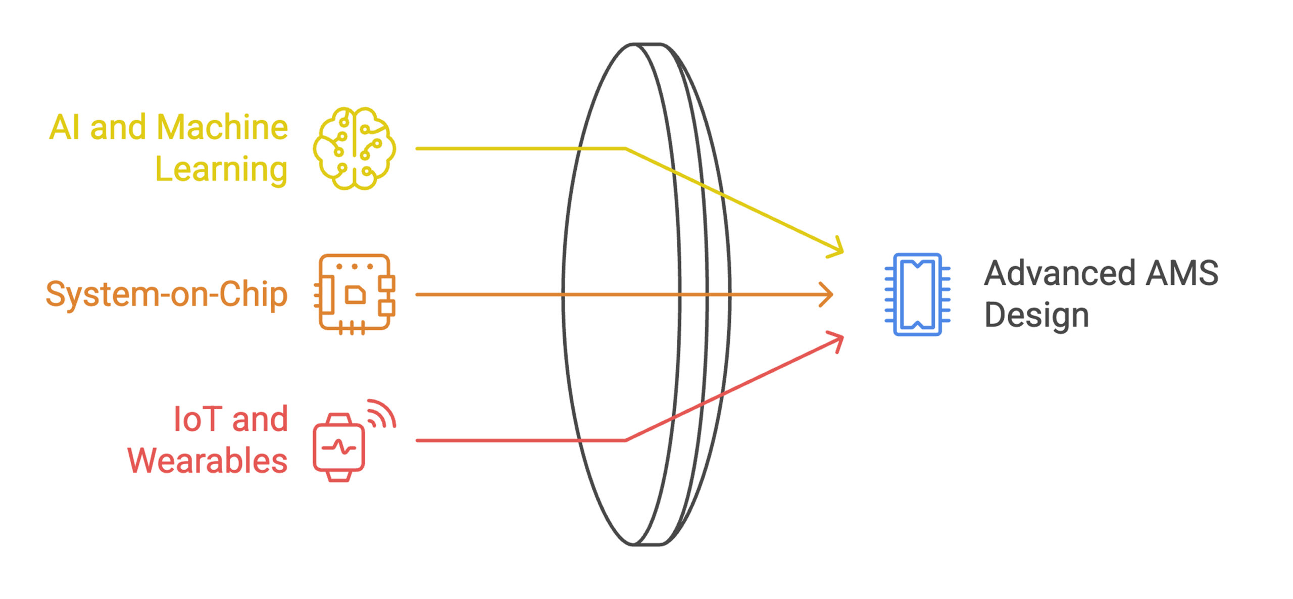
Integration of AI and Machine Learning
AI/ML is revolutionizing mixed signal design by automating tedious tasks and optimizing circuit performance. Generative AI is now being used in Electronic Design Automation (EDA) to predict circuit behavior and automate custom layouts, reducing design cycles by up to 40%. Machine learning algorithms can analyze vast datasets of design parameters and circuit simulations to identify optimal configurations. This can significantly reduce design time and improve circuit performance in areas like:
- For improved performance measures like power consumption, signal-to-noise ratio, and gain, AI may adjust transistor size, biasing conditions, and layout.
- The routing of intricate interconnects within an integrated circuit (IC) may be automated using machine learning techniques, guaranteeing signal integrity and reducing parasitic effects.
- AI can be used to create highly accurate yet efficient simulation models, reducing design verification time.
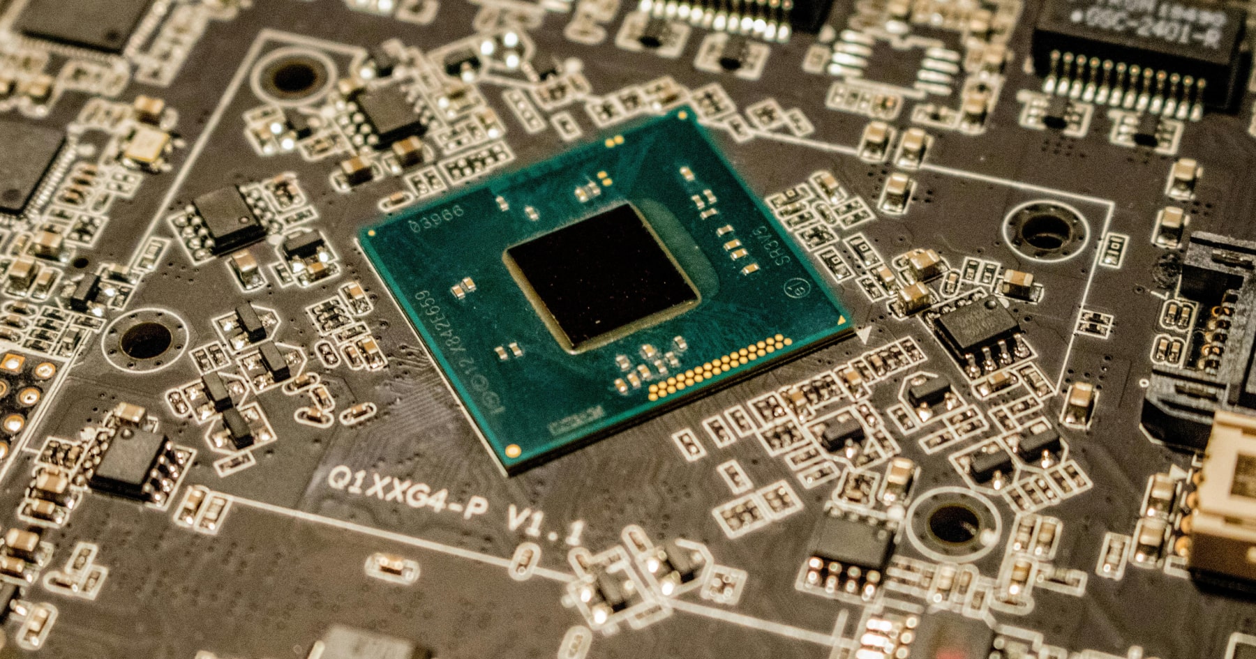
Increased Use of System-on-Chip
SoCs integrate various functionalities like digital processors, memory, analog interfaces, and RF components onto a single chip. This miniaturization offers several advantages:
- SoCs enable the creation of smaller and lighter electronic devices, ideal for wearables and portable electronics.
- By eliminating the need for off-chip communication, SoCs achieve higher processing speeds and lower power consumption.
- Integrating multiple functionalities onto a single chip reduces manufacturing complexity and cost.
SoCs are already ubiquitous in smartphones and other mobile devices. Looking ahead, innovations in SoC technology will likely include:
- Combining different chip fabrication processes, for instance, CMOS for digital and GaN for RF, on a single SoC for optimal performance in specific applications.
- Integrating hardware-based security features within SoCs will be crucial for protecting data in connected devices.
The Rise of IoT and Wearable Technology
The Internet of Things (IoT) and wearable technology sectors are booming, creating a significant demand for low-power, compact, and feature-rich hardware board design. Design considerations for IoT devices include:
- Low Power Consumption: These devices often operate on battery power, necessitating ultra-low-power circuit design techniques.
- Connectivity: AMS designers must integrate efficient communication protocols like Wi-Fi 7 and Bluetooth 6.0 for seamless data transmission.
- Nanopower Circuits: New AMS designs are pushing toward “Nanopower” consumption, allowing devices to remain in deep-sleep modes while consuming mere nanowatts of power.
Innovations in AMS design specifically for wearables include:
- Flexible Substrates: Flexible electronics will enable the creation of comfortable and unobtrusive wearable devices that can conform to the human body.
- Bio-Integrated Circuits: These next-generation ICs will interface directly with biological signals, opening doors for novel medical applications.
Energy Efficiency and Low Power Design
With the growing focus on sustainability and battery life, energy efficiency is a top priority in modern electronics. Innovations in low-power AMS design encompass:
- Advanced Device Technologies: GaN transistors offer superior power efficiency compared to traditional silicon-based devices.
- Power Management Techniques: Circuit design approaches that minimize static power consumption and enable dynamic power gating during periods of inactivity will be crucial.
- Energy Harvesting: Techniques for harvesting energy from the environment, like solar and thermal to power IoT devices will become increasingly important.
Unlocking the Potential of Vehicle Data – Exploring Tessolve’s Tera Edge Solution
The Bottom Line!
The analog and mixed signal device market is expected to undergo significant breakthroughs in the future because of the unwavering focus on performance improvement, energy efficiency, and downsizing. AI and machine learning together have the potential to completely transform mixed signal design, reducing procedures and enhancing efficiency.
System-on-Chip (SoC) technology will be used more often, resulting in smaller, more potent systems with better performance and lower prices. The need for creative PCB hardware design that prioritizes seamless communication and low power consumption will grow as wearable and Internet of Things technology proliferates.
Lastly, the development of innovative materials and methods to reduce power usage will be fueled by the emphasis on energy efficiency. These developments will influence electronics going forward and bring in a period of unheard-of creativity and technical breakthroughs as hardware design keeps changing.
FAQs
1. Can you recommend a mixed-signal IC with low noise performance for audio processing in professional studio equipment?
Cirrus Logic MasterHIFI™ series chips offer 130dB dynamic range, providing the ultra-low noise and high-fidelity required for professional audio.
2. What are analog and mixed-signal ICs used for in automotive electronics?
They manage precision battery monitoring in EVs, power ADAS radar sensors, and regulate energy flow within complex electronic control units.
3. What are the best tools for analog and mixed-signal IC design?
Cadence Virtuoso and Synopsys Custom Compiler lead for enterprise design, while Siemens Tanner and LTspice remain top for cost-effective simulation.
4. How does Tessolve add value to the AMS design process?
Tessolve bridges the gap from “Spec to Silicon” by providing end-to-end design, testing, and validation services using industry-leading EDA tools.