The semiconductor industry is undergoing a paradigm shift. Traditional monolithic System-on-Chip (SoC) designs are giving way to modular architectures that leverage interoperable chiplets. At the heart of this evolution is Universal Chiplet Interconnect Express (UCIe). This open standard defines die-to-die physical, protocol, and software layers, enabling seamless integration of chiplets from different vendors.
By providing high bandwidth, low latency, and power-efficient on-package connectivity, UCIe makes it possible to assemble SoCs like building blocks, accelerating innovation and lowering costs.
Why Chiplets and Why Now?
For decades, Moore’s Law allowed the integration of more transistors into a single die. But as scaling slows and reticle limits make large dies expensive and yield-sensitive, the industry has turned to chiplets.
Here’s why chiplets are gaining momentum:
- Yield and cost benefits: Smaller dies improve yield, reducing manufacturing losses compared to giant monolithic SoCs.
- Heterogeneous integration: Teams can integrate different technologies such as analog, RF, optical, memory, or accelerators within one package.
- Flexibility and scalability: Functions like CPU, GPU, I/O, and accelerators can evolve independently.
- Time-to-market: Reusing proven chiplets shortens design cycles.
Together with advances in packaging and UCIe standardization, these advantages make modular SoC design both feasible and attractive.
What is UCIe?
UCIe (Universal Chiplet Interconnect Express) is an open industry standard that defines how chiplets communicate inside a package. It provides:
- PHY Layer: High-bandwidth, low-power electrical die-to-die signaling
- Protocol Layer: Support for PCIe, CXL, and custom streaming modes
- Software Layer: Standardized discovery, enumeration, and management
- Compliance Framework: Ensures interoperability across vendors
By standardizing these layers, UCIe aims to create a plug-and-play chiplet ecosystem, similar to how PCIe unified board-level connectivity.
Why UCIe Matters in the Chiplet Era
Chiplets require reliable, high-speed, low-power communication, but proprietary die-to-die interfaces create vendor lock-in and high development cost.
UCIe solves these problems by:
- Removing the need for custom interconnects
- Providing predictable bandwidth and latency targets
- Supporting multiple packaging types (organic, 2.5D, 3D)
- Simplifying heterogeneous integration
- Enabling marketplace-style chiplet reuse
This makes UCIe the primary enabler of practical, scalable chiplet-based designs.
Practical Workflow for Modular SoC Design
Designing with chiplets requires a new workflow mindset. Here are four key stages:
1. System Partitioning
Map workloads to specific functions: compute, memory, I/O, accelerators, and security. Decide which blocks require cutting-edge process nodes (like CPUs) and which can use mature nodes (such as analog or I/O). Getting partitioning right early avoids major rework later.
2. Choosing Interfaces and Topologies
UCIe provides standardized die-to-die fabrics. Depending on system requirements, you might adopt hub-and-spoke, mesh, or hierarchical topologies. Memory proximity, latency, and coherence models all play into this decision.
3. Reusable, Portable Chiplets
Each chiplet should be designed as a self-contained module with clear electrical, thermal, and mechanical specifications. Compliance with UCIe ensures smooth integration across vendors.
4. Verification and Bring-Up
Verification must now cover both die-level and package-level interactions. Post-silicon validation, boundary scans, and automated test equipment (ATE) strategies are essential for debugging at scale.
Top-Level Chiplet Architecture Using UCIe
The diagram below illustrates a typical modular SoC architecture, showing CPU, GPU, Accelerator, and Memory chiplets connected via UCIe die-to-die links.
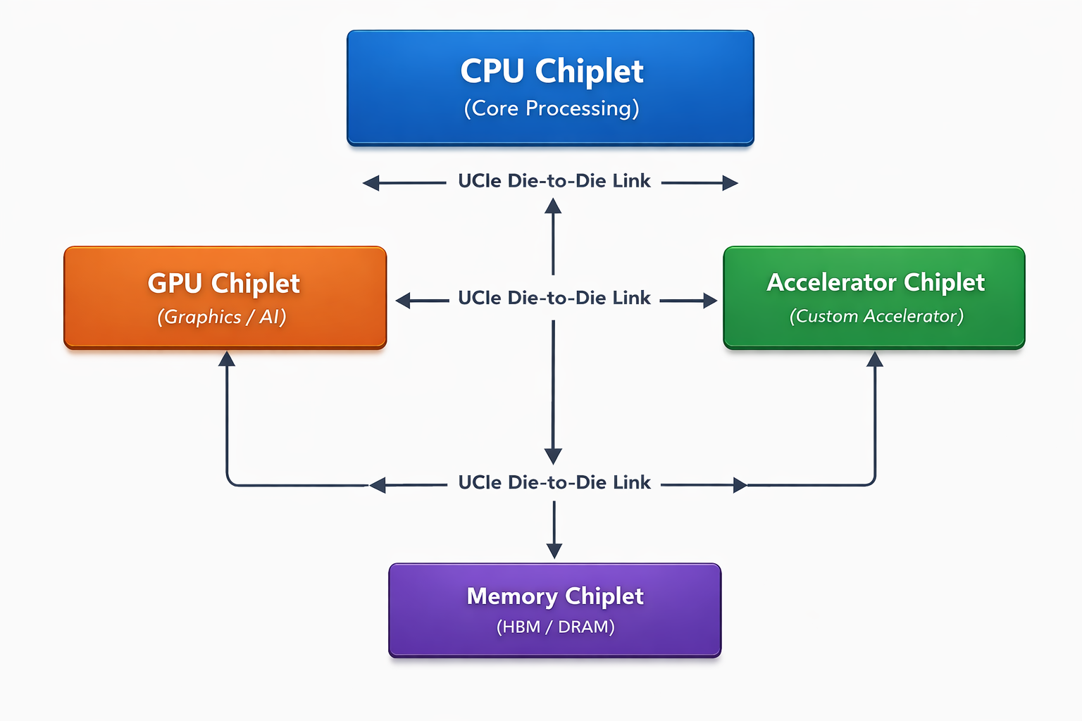
Figure: Top-level modular SoC using UCIe die-to-die connectivity. CPU, GPU, Accelerator, and Memory chiplets communicate via high-bandwidth, low-latency UCIe links.
As shown above, the CPU acts as the central hub, linking to GPU and accelerator chiplets, while memory chiplets connect to all components. This setup supports scalable, modular, and heterogeneous integration.
The Role of Packaging in Modular SoCs
Advanced packaging technologies such as 2.5D interposers, fan-out wafer-level packaging (FOWLP), and 3D stacking are essential for chiplet integration. These techniques not only connect dies electrically but also manage heat dissipation, mechanical stress, and overall system reliability. In modular SoCs, packaging is no longer a “back-end” task but a co-design activity alongside chip design. Choosing the right packaging approach ensures optimal signal integrity, power delivery, and thermal management, all of which determine system performance. For companies exploring chiplets, close collaboration with a packaging-aware chip design company is critical.
UCIe Pros and Cons
Pros
- High-bandwidth, low-latency die-to-die communication
- Multi-vendor interoperability through compliance testing
- Supports PCIe, CXL, and custom streaming modes
- Scalable from mobile SoCs to HPC accelerators
- Power-efficient compared to off-package interfaces
- Enables modular design and faster product iteration
Cons
- Standard is still evolving; early versions have limitations vs. proprietary PHYs
- Requires packaging-aware RTL and physical design
- Multi-die testing complexity increases dramatically
- Thermal hotspots around UCIe PHY blocks
- Limited tool and IP maturity for some foundry nodes
UCIe Implementation Challenges
Integrating UCIe into a product requires deep technical alignment across the design flow:
RTL Level
- Integration of the UCIe controller IP
- Training FSMs, CRC logic, flow control
- Protocol wrappers (PCIe/CXL/streaming mode)
Synthesis / Netlist
- Multi-clock-domain timing closure
- Pipe stages to meet PHY timing
Floorplanning
- UCIe PHY must be placed at specific die edges
- Routing escape paths to microbumps
- Thermal-aware placement
Place & Route
- Tight timing constraints around PHY to logic
- Power grid design for high-speed PHYs
Signoff & GDS
- Package co-simulation (SI, thermal, EM/IR)
- Alignment accuracy between dies
- Reliability verification for dense microbump arrays
DFT & Test
- UCIe-specific BIST
- Boundary scan for multi-die
- Known Good Die (KGD) workflows
- ATE bring-up of UCIe links
This is the core engineering effort behind successful UCIe products.
Design Considerations and Pitfalls
While chiplets offer compelling benefits, they also introduce challenges:
- Thermal & Power Delivery: Multiple dies increase the risk of hotspots and complicate power distribution.
- Signal Integrity: High-speed UCIe lanes require careful package co-design.
- Interoperability: Without compliance testing, integration issues can arise between chiplets from different vendors.
- Security: Chiplets sourced from various suppliers require robust supply-chain validation and secure boot mechanisms.
Mitigating these risks demands strong engineering discipline and proven chip design expertise.
Tools and Ecosystem Support
The ecosystem around UCIe and chiplets is maturing quickly:
- EDA tools now support multi-die floorplanning and UCIe-aware package co-simulation
- UCIe Consortium offers compliance test suites and reference models
- Vendors and foundries are introducing UCIe-compatible chiplets
For scalable adoption, collaboration with a trusted chip design company ensures seamless alignment across design, packaging, and test flows.
Checklist for Getting Started with Chiplets
If you’re considering modular SoC design, keep this checklist handy:
- Define performance targets and partition functions.
- Select UCIe-compatible chiplet vendors and packaging partners.
- Create a verification plan covering die and package levels.
- Allocate power, thermal, and mechanical budgets early.
- Build in supply-chain security and provenance tracking.
Extended Applications of Chiplets
Chiplet-based SoCs are accelerating innovation across data centers, mobile devices, automotive, AR/VR, and more. UCIe provides the unified foundation enabling these systems to scale efficiently, improve modularity, and support heterogeneous integration.
Real-World Momentum
Leading companies have begun adopting UCIe for cloud computing, HPC, and AI acceleration. Research continues into optical UCIe PHYs and next-generation packaging, signaling a strong future for UCIe-based products.
UCIe is not just theoretical; it is already shaping the next generation of semiconductor designs.
Tools, Technology, and Intelligent Automation
Modern validation relies on advanced platforms like Advantest and Teradyne ATE systems, precision probing, custom load boards, and comprehensive characterization setups. These tools allow engineers to push devices to their operational limits under carefully controlled conditions. Environmental chambers test temperature extremes while automated infrastructure accelerates throughput without compromising quality.
Equally important is the software side. Today’s frameworks bring together program development environments, debug utilities, analytics dashboards, and real-time reporting systems. Together, they unlock deeper insights, improve decision-making, and dramatically reduce time to market. When executed well, test engineering is as much about intelligence as it is about instrumentation.
Talent at the Heart of Innovation
Advanced tools are essential, but exceptional talent makes the real difference. Modern test engineering requires engineers who can seamlessly combine knowledge of silicon physics, system behavior, automation frameworks, firmware integration, and data analytics. Collaboration across disciplines is just as critical as technical skill. Teams that balance creativity, precision, and cross-functional expertise are driving the development of reliable, production-ready technology and setting new standards for system-level quality.
From SoCs to Multi‑Die Architectures: A Practical Guide to 3D IC Design
Tessolve: Your Partner in Chiplet and Modular SoC Design
At Tessolve, we bring modular SoC ideas to life. As a global engineering services provider, we deliver end-to-end chip design, validation, and test solutions. Our expertise spans design services, post-silicon validation, test engineering, PCB and system design, and scalable test-lab infrastructure.
We help customers adopt chiplet and UCIe-based architectures by providing packaging-aware design, compliance testing, and robust post-silicon debug. As a trusted chip design company, we combine innovation with proven engineering practices to accelerate time-to-market. For businesses seeking reliable, future-ready chip solutions, Tessolve is the partner of choice.