In the realm of high-speed electronics, the design of printed circuit boards (PCBs) has evolved into a sophisticated discipline where precision is paramount. As data rates escalate and electronic systems become more complex, ensuring the integrity of signals and the stability of power delivery becomes increasingly challenging. This is where Signal Integrity (SI) and Power Integrity (PI) co-simulation emerges as a critical tool in the arsenal of PCB designers, aiming to mitigate post-fabrication surprises and ensure optimal performance.
Understanding SI/PI Co-Simulation
Signal Integrity (SI) refers to the quality of electrical signals as they traverse the PCB, ensuring that they maintain their intended shape and timing. Factors such as impedance mismatches, crosstalk, ground bounce, and reflections can degrade signal quality, leading to errors and system instability.
Power Integrity (PI) focuses on the stable delivery of power to all components on the PCB. Issues like voltage drops, excessive ripple, and switching noise can compromise the power supply, affecting the system’s performance and reliability.
SI/PI co-simulation involves the simultaneous analysis of both signal and power integrity within a unified simulation environment. This holistic approach allows designers to identify and address potential issues early in the design process, reducing the risk of costly revisions and ensuring that the final product meets performance specifications.
Why Traditional Approaches Fall Short
In traditional PCB design workflows, SI and PI are often treated as separate concerns, with different engineers handling each domain independently. While this approach may work for slower-speed applications, it becomes inadequate in high-speed designs where signal and power domains are tightly coupled. For example, switching currents from high-speed digital circuits can inject noise into the power delivery network, which in turn degrades signal quality.
This fragmented view leads to blind spots that are only discovered after fabrication, often requiring costly redesigns. With SI/PI co-simulation, engineers can visualize these interactions and take preventive measures from the start.
High-Density Interconnect (HDI) PCB Design: Best Practices for Complex Products
The Importance of SI/PI Co-Simulation in High-Speed PCB Design
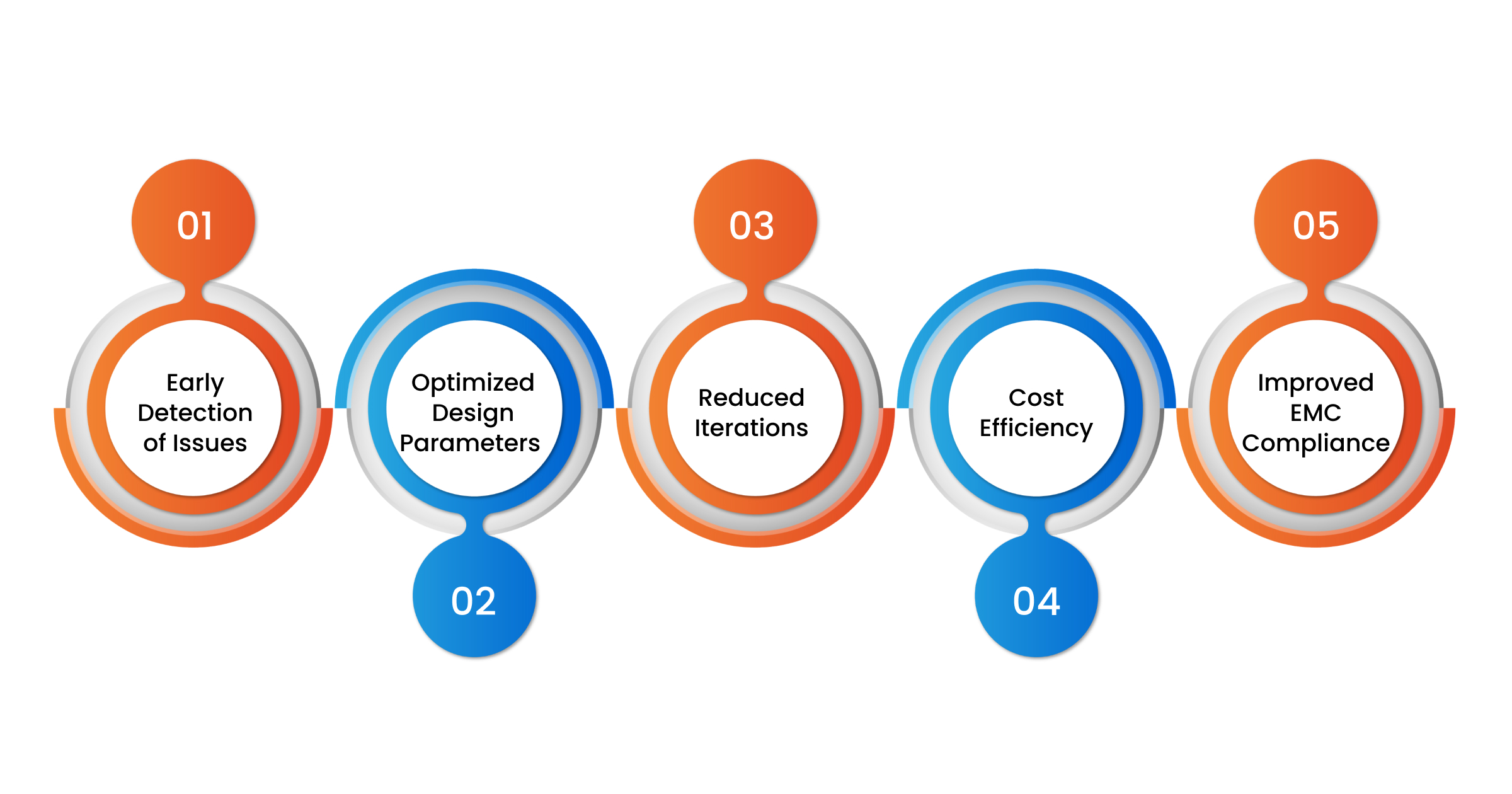
- Early Detection of Issues: By simulating both signal and power integrity concurrently, designers can identify potential problems such as voltage fluctuations affecting signal quality or signal transitions causing power noise. This proactive approach enables timely corrections before fabrication.
- Optimized Design Parameters: Co-simulation allows for the fine-tuning of design parameters, such as trace widths, spacing, and layer stack-ups, to achieve optimal performance. This ensures that the PCB operates reliably under various conditions.
- Reduced Iterations: Traditional design approaches might require multiple iterations to resolve SI and PI issues separately. Co-simulation streamlines this process, reducing the number of design cycles and accelerating time-to-market.
- Cost Efficiency: Identifying and resolving issues during the design phase is significantly more cost-effective than post-fabrication fixes. Co-simulation minimizes the risk of rework, saving both time and resources.
- Improved EMC Compliance: Electromagnetic compatibility (EMC) is a growing concern in high-speed designs. SI/PI co-simulation helps in predicting and mitigating EMI issues before they become regulatory roadblocks.
Implementing SI/PI Co-Simulation: Best Practices
- Integrated Design Tools: Utilize simulation tools that support co-simulation, enabling seamless analysis of SI and PI within the same environment. This integration facilitates a more comprehensive understanding of the interactions between signals and power delivery.
- Accurate Modeling: Ensure that models for components, interconnects, and power delivery networks are accurate and reflect real-world behavior. This accuracy is crucial for reliable simulation results.
- Cross-Disciplinary Collaboration: Encourage collaboration between signal integrity engineers, power integrity specialists, and layout designers. A multidisciplinary approach ensures that all aspects of the design are considered holistically.
- Iterative Validation: Perform simulations at various stages of the design process, from initial concept to final layout. Iterative validation helps in catching issues early and refining the design progressively.
- Design Rule Enforcement: Using SI/PI co-simulation results to refine design rules can lead to systemic improvements across multiple projects, improving overall PCB hardware design workflows.
Download Brochure
Hardware Brochure
Tessolve provides turnkey PCB solutions from schematic design to layout to thoroughly tested assembly
Case Study PDF Download
The Role of Professional Services in SI/PI Co-Simulation
Engaging with a reputable PCB design company that offers comprehensive PCB design services can significantly enhance the effectiveness of SI/PI co-simulation. These companies bring expertise, advanced tools, and proven methodologies to the table, ensuring that the PCB hardware design meets the highest standards of performance and reliability.
Partnering with specialists also ensures you stay ahead of technological advancements. With newer chipsets pushing the limits of speed and power, only a co-simulation approach can future-proof your design strategy.
Tessolve: Your Partner in High-Speed PCB Design
Tessolve understands the complexities involved in high-speed PCB design boards and the critical role that SI/PI co-simulation plays in ensuring their success. Our dedicated team of over 250 design engineers specializes in delivering end-to-end PCB design services, from schematic capture to fully tested assembled boards.
We leverage advanced simulation tools and methodologies to perform thorough SI/PI analysis, identifying potential issues early in the design process. Our holistic approach ensures that both signal and power integrity are optimized, reducing the risk of post-fabrication surprises.
As a leading PCB design company, Tessolve is committed to delivering high-quality PCB hardware designs that meet the stringent demands of modern electronic systems. Our experience spans across sectors including automotive, aerospace, industrial, and medical, making us the ideal partner for any high-speed application. Partner with us to experience the difference that expert SI/PI co-simulation can make in your next project.
Optimizing Your PCB Design: A Guide to Stackup Selection
Conclusion: Future-Proof Your PCB with SI/PI Co-Simulation
As devices become faster and more compact, traditional PCB design methods struggle to meet the demands of performance, reliability, and compliance. SI/PI co-simulation is no longer a luxury; it’s a necessity in high-speed PCB design. It allows engineers to holistically evaluate how signals interact with power delivery networks and vice versa, leading to more robust and reliable outcomes.
By adopting SI/PI co-simulation early in the design process, companies can reduce post-fabrication surprises, eliminate unnecessary iterations, and accelerate their product development timelines. When paired with the expertise of a trusted PCB design company like Tessolve, the benefits multiply, ensuring that every PCB design board not only meets but exceeds industry standards.
If you’re looking to future-proof your product, reduce development risks, and improve time-to-market, consider integrating SI/PI co-simulation into your PCB design service strategy. With technologies evolving rapidly, only those who adopt a comprehensive, simulation-driven approach will lead the next generation of electronic innovation.