The semiconductor industry is undergoing a major shift, with High-Performance Computing (HPC) and AI driving new advancements. At the heart of this evolution are heterogeneous packaging and chiplet-based architectures, which enable the integration of multiple process nodes to create powerful, scalable, and energy-efficient solutions. While these innovations open new possibilities, they also bring unprecedented challenges—particularly in testing.
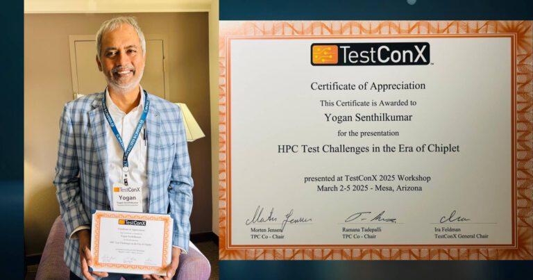
At TestConX 2025, Yogan Senthilkumar, Vice President of Engineering at Tessolve, shared his expertise on the evolving landscape of HPC test challenges in the chiplet era. With over 35 years of experience in semiconductor testing, Yogan provided a deep dive into the critical factors influencing chiplet-based SoC deployment and the solutions needed to address them.
Key Takeaways from the Presentation
Thermal Management: A Crucial Factor in HPC Testing
One of the biggest challenges in testing HPC chiplets is thermal management. As chiplets continue to push the boundaries of power density, thermal runaway can have a serious impact on both performance and reliability. Effective thermal strategies aren’t just essential for package design—they also play a vital role in ensuring long-term functionality, especially at scale.
For large-scale HPC deployments, managing thermal efficiency is also a step toward reducing the overall carbon footprint. The demand for more powerful AI and HPC systems means that optimizing cooling solutions and power management is no longer optional—it’s a necessity.
The Need for Known-Good-Die (KGD) and Optimized Test Yields
Heterogeneous integration means that every chiplet, including DDR, PMICs, and other supporting ICs, must meet strict Known-Good-Die (KGD) standards. Unlike traditional monolithic SoCs, chiplet architectures introduce additional layers of complexity when it comes to test coverage and defect isolation. Ensuring that each die is fully functional before integration is critical to minimizing yield loss and optimizing production efficiency.
Yogan emphasized that a strong final test strategy directly impacts cost efficiency and product reliability. Without a well-planned test approach, defects in even a single chiplet can lead to costly failures at the system level.
Addressing the Complexities of Chiplet-Based SoC Testing
Testing chiplets differs significantly from testing monolithic SoCs, as it requires a new set of methodologies to account for multi-die integration. Some of the key areas that need to be addressed include:
- Interconnect Reliability: Ensuring seamless communication between chiplets, with a focus on signal integrity and electrical performance.
- Comprehensive Test Coverage:Managing variations in process nodes and ensuring uniform quality across all integrated components.
- System-Level-Test a key for HPC / AI products: Moving beyond traditional functional tests to evaluate real-world performance before deployment.
By adopting a holistic approach to testing, semiconductor companies can mitigate risks and improve the overall robustness of chiplet-based designs.
Also Read: The Promise of Quantum Computing and its Impact on Chip Design
Tessolve: Driving Innovation in Semiconductor Testing
At Tessolve, we specialize in solving the toughest semiconductor test challenges. With deep expertise in test engineering, silicon validation, reliability analysis, and ATE solutions, we enable our customers to develop high-quality, high-yield products with confidence.
Yogan’s insights at TestConX 2025 reaffirm our leadership in advancing HPC and AI test methodologies. As semiconductor complexity continues to grow, we remain committed to pushing the boundaries of innovation, helping customers navigate the transition to chiplet-based architectures with efficiency and reliability.
Want to explore how Tessolve’s cutting-edge test solutions can support your next-generation semiconductor designs? Connect with our experts today!