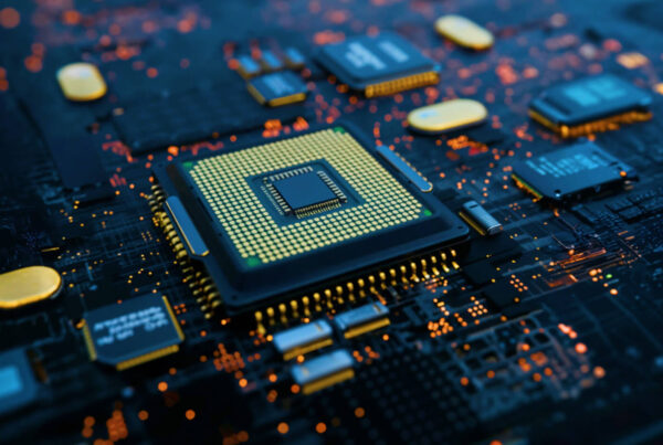
In an era dominated by compact electronics and advanced functionality, the need for highly efficient printed circuit boards is more crucial than ever. High-Density Interconnect (HDI) technology has emerged as a preferred solution for developing miniaturized and performance-driven electronic products. From smartphones to aerospace equipment, HDI PCBs are central to complex system designs where traditional boards fall short.
To design successful HDI boards, engineers must navigate multilayer stack-ups, tight tolerances, and fine-pitch components. This article explores the best practices for HDI PCB development and how leveraging expert PCB design service providers can make a critical difference.
What Is HDI PCB and Why Is It Important?
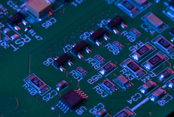
HDI PCBs are characterized by their high wiring density per unit area. They incorporate microvias, blind/buried vias, and sequential lamination processes to achieve enhanced performance in a compact footprint. These boards support advanced features such as:
- Faster signal transmission
- Better electromagnetic compatibility (EMC)
- Lower power consumption
- Reduced size and weight
Due to their ability to integrate more components into smaller areas, HDI PCBs are essential in industries such as consumer electronics, automotive, aerospace, and medical devices.
Challenges in HDI PCB Design
While HDI PCBs offer many advantages, they also introduce a new level of design complexity. Common challenges include:
- Limited space for routing: With denser layouts, there’s minimal room for trace routing.
- Signal integrity issues: High-speed signals can experience degradation due to impedance mismatches.
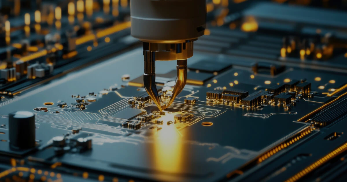
- Manufacturing constraints: Fabrication of microvias and multiple lamination cycles require tight process control.
- Cost: Advanced materials and processes make HDI boards more expensive.
This is where a professional PCB design service becomes vital. Outsourcing to experienced partners ensures designs meet both performance and manufacturability standards.
Best Practices for HDI PCB Design
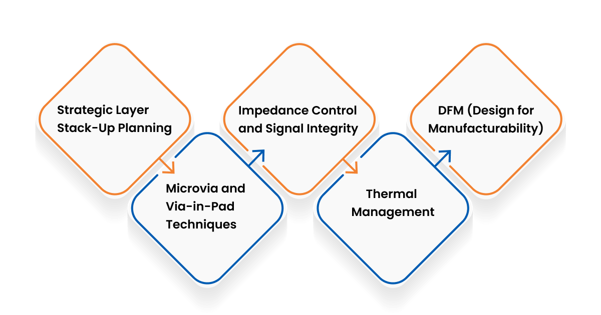
1. Strategic Layer Stack-Up Planning
Effective stack-up design is the cornerstone of any HDI board. Aim to:
- Use symmetrical layer stacks to reduce warpage.
- Alternate signal and ground/power planes for controlled impedance.
- Position high-speed signals closer to reference planes.
When planning layer stacks, collaborate closely with your PCB design engineer to define layer count, dielectric thickness, and via structures.
2. Microvia and Via-in-Pad Techniques
Microvias enable interconnections between layers with minimal board real estate. To optimize them:
- Use laser drilling for accuracy and reliability.
- Keep microvia aspect ratios below 1:1.
- Consider stacked or staggered microvias based on the routing need.
Via-in-pad is another space-saving method, often necessary for fine-pitch BGA components. Ensure proper via filling and plating to avoid soldering issues.
3. Impedance Control and Signal Integrity
Signal integrity becomes a major concern with dense HDI layouts. Best practices include:
- Use controlled impedance traces with proper width and spacing.
- Avoid 90-degree bends to reduce reflections.
- Use differential pair routing for high-speed signals.
Partnering with a knowledgeable PCB hardware design provider ensures thorough pre-layout and post-layout signal integrity analysis.
4. Thermal Management
Miniaturization leads to heat concentration in small areas. To manage thermal performance:
- Use thermal vias to dissipate heat from hotspots.
- Select high-Tg and low-CTE materials.
- Distribute power and ground planes uniformly to reduce temperature rise.
Effective thermal planning is integral to long-term board reliability and is often integrated into comprehensive PCB solution strategies.
5. DFM (Design for Manufacturability)
Since HDI fabrication is more complex, incorporating DFM guidelines early helps reduce costs and production delays. Follow these DFM practices:
- Adhere to the fabricator’s minimum trace width/spacing.
- Minimize the number of lamination cycles.
- Use standardized pad sizes for ease of assembly.
A skilled PCB design engineer will integrate DFM rules into the layout process to ensure your design is both functional and manufacturable.
Designing for 5G: PCB Considerations for Next-Generation Connectivity
CAD Tools and Simulation
Modern HDI design relies heavily on powerful EDA tools for simulation, layout, and verification. Tools like Altium Designer, Cadence Allegro, and Mentor Graphics support HDI-specific features such as:
- Blind/buried via implementation
- Auto-routing of dense BGAs
- Impedance calculators and stack-up editors
Advanced simulation features also help detect crosstalk, EMI, and power integrity issues—well before production.
Importance of Working with an Expert PCB Design Partner
HDI projects demand cross-functional expertise in electrical, mechanical, and thermal domains. A holistic PCB solution should cover:
- Design consultation
- Signal and power integrity analysis
- Prototype fabrication and testing
- Mass production support
That’s why many companies choose to work with end-to-end PCB design service providers that offer multi-disciplinary expertise and global manufacturing networks.
Download Brochure
Hardware Brochure
Tessolve provides turnkey PCB solutions from schematic design to layout to thoroughly tested assembly
Case Study PDF Download
Future Trends in HDI Technology
As demand for smaller, faster, and smarter devices increases, HDI PCBs will continue evolving. Emerging trends include the use of embedded components, advanced materials like liquid crystal polymers (LCP), and integration with 3D packaging. Staying ahead in PCB hardware design means keeping pace with these innovations to deliver cutting-edge, compact, and reliable electronic products.
Why Choose Tessolve for HDI PCB Design?
Tessolve brings a full-spectrum approach to PCB hardware design, ensuring performance, scalability, and reliability from concept to product realization. With experience handling over 3000 board designs—including high-speed HDI, rigid-flex, and mixed-signal systems—our team is equipped with the latest tools and methodologies. As a trusted PCB design service partner to Fortune 500 companies, Tessolve supports complex requirements in automotive, industrial, aerospace, and telecom sectors. Our global design centers and labs provide rapid prototyping, testing, and compliance—all under one roof. When you work with Tessolve, you’re not just getting a PCB design engineer, but a complete PCB solution tailored to your product’s needs.
Optimizing Your PCB Design: A Guide to Stackup Selection
Let’s Conclude
As electronic systems grow more complex and compact, High-Density Interconnect (HDI) technology has become indispensable. Successfully designing HDI boards requires precision, experience, and advanced tools. By following best practices—such as strategic layer stack-up, proper via design, and DFM integration—you can overcome the challenges and leverage HDI’s full potential.
Whether you’re developing consumer gadgets or mission-critical devices, the right PCB design service partner can accelerate innovation while minimizing risk. Investing in experienced PCB design engineer support and end-to-end PCB solution services is no longer optional—it’s a competitive necessity.