When it comes to complex electronics, high-density printed circuit boards (PCBs) are at the heart of advanced systems from automotive controllers to telecom infrastructure and high-speed computing solutions. As transistor counts soar and trace densities increase, managing electrical noise, especially Simultaneous Switching Noise (SSN), becomes a critical requirement in the PCB hardware design process.
In this blog, we’ll explain what an SSN is, why it matters in high-density boards, and how thoughtful hardware engineering practices help mitigate it.
Understanding Simultaneous Switching Noise in High-Density PCB Hardware
High-density PCBs pack many layers, signals, and components into a compact footprint. While this enables powerful, space-efficient designs, it also creates electrical characteristics that differ significantly from simpler boards. One of the most challenging phenomena in such environments is Simultaneous Switching Noise (SSN), also known as ground bounce. SSN arises when multiple digital outputs switch states at the same time, causing abrupt changes in current demand that induce noise across the power and ground planes of a PCB.
From a hardware perspective, SSN manifests when fast switching currents create transient voltage fluctuations. These are caused by parasitic inductances and capacitances in the Power Distribution Network (PDN) and the board’s physical layout. In dense designs with high-speed interfaces, these currents and their associated noise become more pronounced, creating challenges for both signal integrity and power integrity.
Why SSN Matters in PCB Hardware Design
- Signal integrity degradation: SSN can introduce timing errors, increased jitter, and potential misinterpretation of logic levels in high-speed signals.
- Power delivery instability: The PDN may experience voltage dips and spikes that affect device operation, particularly at low supply voltages and high current rates.
- Electromagnetic emissions: Transient currents and voltage fluctuations can elevate radiated emissions, complicating electromagnetic compatibility (EMC) compliance.
For designers tasked with creating HDI PCBs (high-density interconnect designs), SSN is not just an academic concept; it’s a practical noise source that must be addressed early in the hardware design cycle.
Mitigation Strategies in PCB Hardware Engineering
Addressing SSN effectively requires both theoretical understanding and practical hardware engineering solutions. Here are key approaches used in professional PCB hardware design:
1. Precision Power Distribution and Grounding
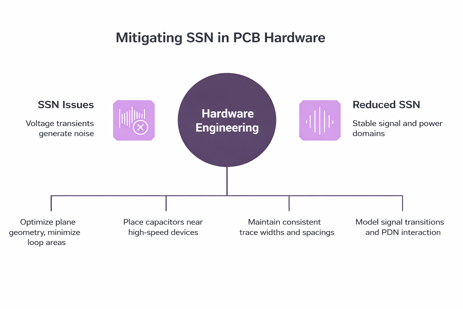
A well-designed power delivery network lays the foundation for controlling SSN. Reducing inductance in the PDN by optimizing plane geometry and minimizing loop areas helps limit the voltage transients that generate noise. Pairing this with a robust ground reference plane is essential to maintain stable signal and power domains.
2. Strategic Use of Decoupling
Decoupling capacitors are a fundamental tool in SSN mitigation. By placing capacitors of appropriate values between the power and ground planes near high-speed devices, transient currents are supplied locally, reducing the impact of sudden switching on the PDN.
3. Controlled Impedance Routing and Stack-Up Design
In high-density PCB hardware design, trace widths and spacings are controlled to maintain consistent impedance. This reduces reflections and minimizes the interaction between signal transitions and power-plane noise. Carefully planned layer stack-ups also help segregate power and signal layers to improve both signal integrity and power integrity.
4. SI/PI Co-Simulation in Design Validation
Advanced simulation techniques play a crucial role in evaluating potential SSN issues before fabrication. SI (Signal Integrity) and PI (Power Integrity) co-simulation allows engineers to model and visualize how signal transitions and PDN characteristics interact. This enables proactive adjustments, such as rebalancing trace placement or tuning decoupling strategies, long before boards go into production.
By integrating co-simulation into the design workflow, engineers save time, reduce the risk of costly revisions, and increase first-pass success rates in production.
High-Density Interconnect (HDI) PCB Design: Best Practices for Complex Products
Tessolve’s Advanced PCB Hardware Design Capabilities
At Tessolve, we understand that managing SSN and other electrical noise challenges is integral to delivering high-reliability boards. Our hardware engineering solution services are structured to address these complexities from schematic capture through layout and simulation, all the way to tested hardware delivery.
Tessolve’s offerings in PCB hardware design encompass:
- Schematic Capture and Library Development: Ensuring accurate representation of circuits and component footprints that conform to industry standards.
- Layer Stack-Up and Layout Design: Creating optimized high-density designs that balance functionality, performance, and manufacturability.
- Signal and Power Integrity Simulation: Using industry-standard EDA tools to perform SI/PI analysis that identifies potential noise issues, including SSN, and enables design refinements.
- Design Rule Validation and DFM Checks: Applying in-house CAM engineering and validation routines to ensure manufacturability and compliance with IPC and customer standards.
- Comprehensive Hardware Engineering Solutions: Integrated services that cover high-speed digital, mixed-signal, RF, and HDI designs for sectors such as automotive, semiconductor, industrial, and consumer electronics.
By combining leading-edge tools with experienced hardware engineers, Tessolve helps customers mitigate electrical noise issues like SSN early and efficiently.
Frequently Asked Questions (FAQs)
1. What exactly is Simultaneous Switching Noise (SSN) in PCB design?
Simultaneous Switching Noise refers to transient voltage fluctuations that occur when multiple digital outputs switch states at the same time, causing current surges that can perturb both the power distribution network and signal lines.
2. Why is SSN a concern in high-density PCBs?
High-density PCBs pack more components and signals close together, increasing the likelihood that multiple circuits will switch simultaneously. This amplifies noise effects, complicates signal integrity, and may lead to timing errors or data corruption if not properly managed.
3. How does PI/PDN optimization help reduce SSN?
Optimising the power distribution network by minimising inductance and using appropriate decoupling capacitors reduces transient voltage swings caused by switching events, directly mitigating SSN impact.
4. What role does co-simulation play in managing SSN?
SI/PI co-simulation allows hardware designers to analyse signal and power integrity simultaneously, identifying interactions that can cause noise issues like SSN and enabling corrective actions before fabrication.
5. Can hardware engineering solutions alone eliminate SSN entirely?
While careful hardware engineering and design practices significantly reduce SSN, completely eliminating it depends on multiple factors, including board complexity, operating speed, and system requirements. Effective design and simulation, as part of a hardware engineering solution, minimise its impact in real-world applications.