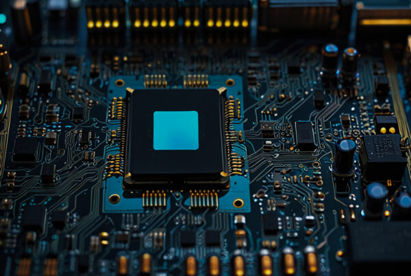
Creating an AI System-on-Chip (SoC) today resembles conducting a thousand musicians playing different melodies at once; each note, or data stream, must align perfectly. As AI workloads become increasingly complex, prototyping these SoCs on FPGA (Field Programmable Gate Array) platforms has become an essential step for verifying architectures before committing to silicon.
FPGA prototyping offers flexibility, speed, and scalability that traditional simulation just can’t match. But when you’re dealing with massive parallelism, multiple processing clusters, and terabytes of bandwidth, “just mapping it on an FPGA” isn’t as simple as it sounds.
So let’s talk about what it really takes to build scalable FPGA prototypes for modern AI SoCs, and how to keep your sanity while doing it.
Why FPGA Prototyping Matters for AI SoCs
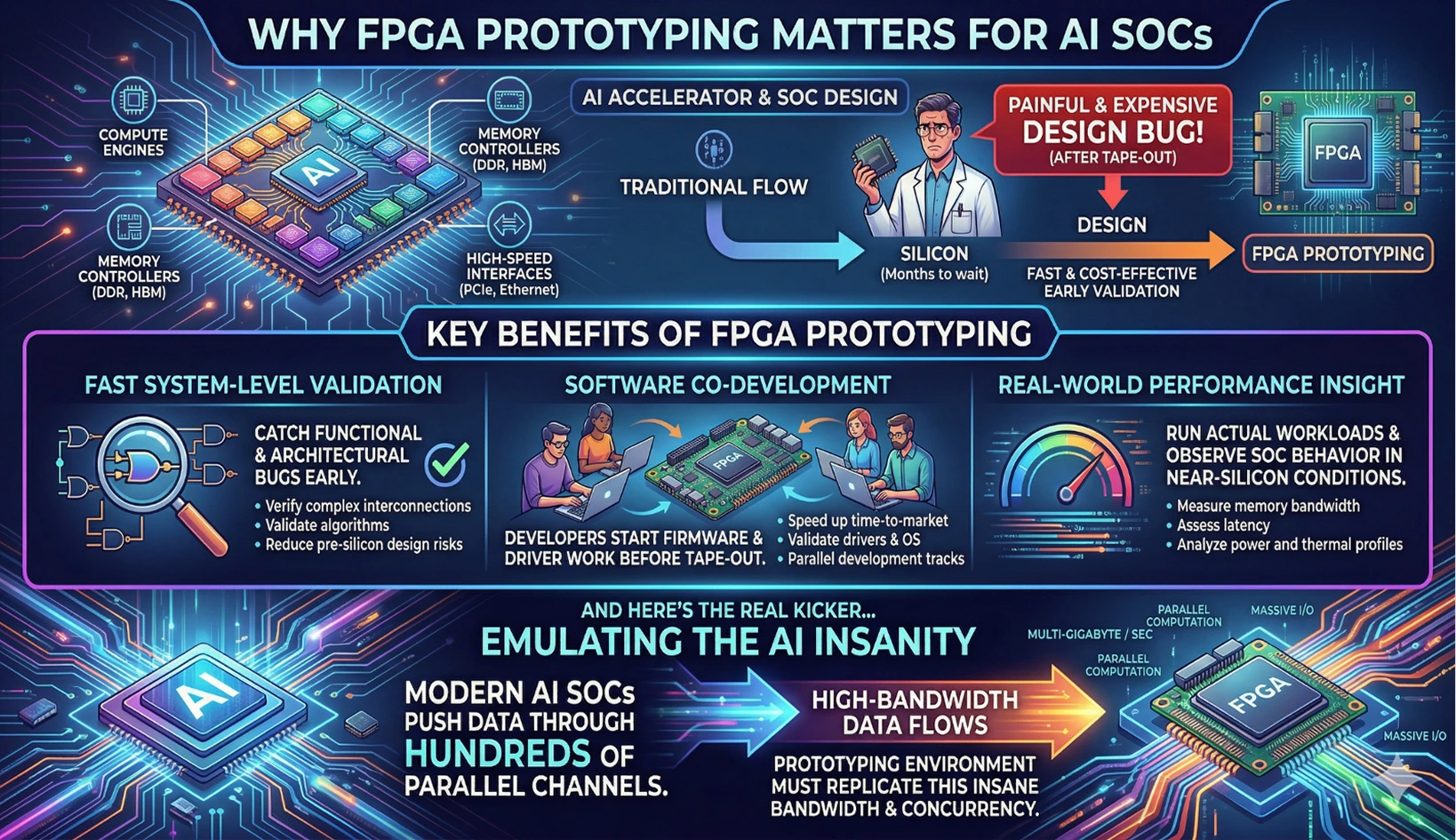
AI accelerators and SoCs integrate dozens of compute engines, memory controllers, and high-speed interfaces. Waiting months for silicon just to realize a design bug is painful (and expensive). That’s where FPGA-based prototyping steps in.
Key Benefits of FPGA Prototyping
- Fast system-level validation: Catch functional and architectural bugs early.
- Software co-development: Developers can start firmware and driver work even before tape-out.
- Real-world performance insight: Run actual workloads and see how the SoC behaves in near-silicon conditions.
And here’s the real kicker: modern AI SoCs push data through hundreds of parallel channels. That means the prototyping environment must replicate this insane bandwidth and concurrency.
The Challenge of Massive Parallelism
AI SoCs aren’t simple pipelines anymore. They’re multi-core, multi-threaded data monsters. Neural network layers, tensor engines, and DMA channels all run in parallel.
What Makes It Hard
- Interconnect explosion: With so many cores, buses, and fabrics can get congested fast.
- Timing closure: Meeting setup and hold across multiple FPGAs is like taming chaos.
- Synchronization: Parallel modules must share data coherently without latency buildup.
Scalable FPGA prototyping needs more than just mapping RTL to logic blocks. You need intelligent partitioning, well-planned clock domains, and efficient data movement strategies.
Partitioning: The Heart of Scalable FPGA Prototyping
If there’s one thing that makes or breaks multi-FPGA prototypes, it’s partitioning. You can’t cram an entire AI SoC into a single FPGA, at least, not without sacrificing realism.
Smart Partitioning Tips
- Group modules by communication frequency. Keep high-traffic blocks close to minimize inter-FPGA traffic.
- Balance logic and memory usage. Don’t let one FPGA run out of LUTs while another sits idle.
- Use modular design flows. This helps maintain consistency when the architecture changes (and it will).
Good partitioning mirrors how you’d approach a custom chip design: balance performance, latency, and resource constraints across the system.
High-Speed Interconnects: Feeding the Beast
Bandwidth is the lifeblood of AI accelerators. When moving workloads across multiple FPGAs, interconnects can easily become bottlenecks.
Ways to Handle Bandwidth in Multi-FPGA Prototyping
- Use high-speed serial links (SERDES): Essential for maintaining throughput without blowing up pin count.
- Leverage time-division multiplexing (TDM): Share communication links efficiently among multiple data streams.
- Buffer wisely: Use FIFOs or asynchronous bridges to manage timing mismatches.
Managing bandwidth isn’t just a technical challenge; it’s an art form. Optimizing it early can dramatically improve final silicon efficiency in your chip design flow.
Memory Hierarchy and Data Flow Modeling
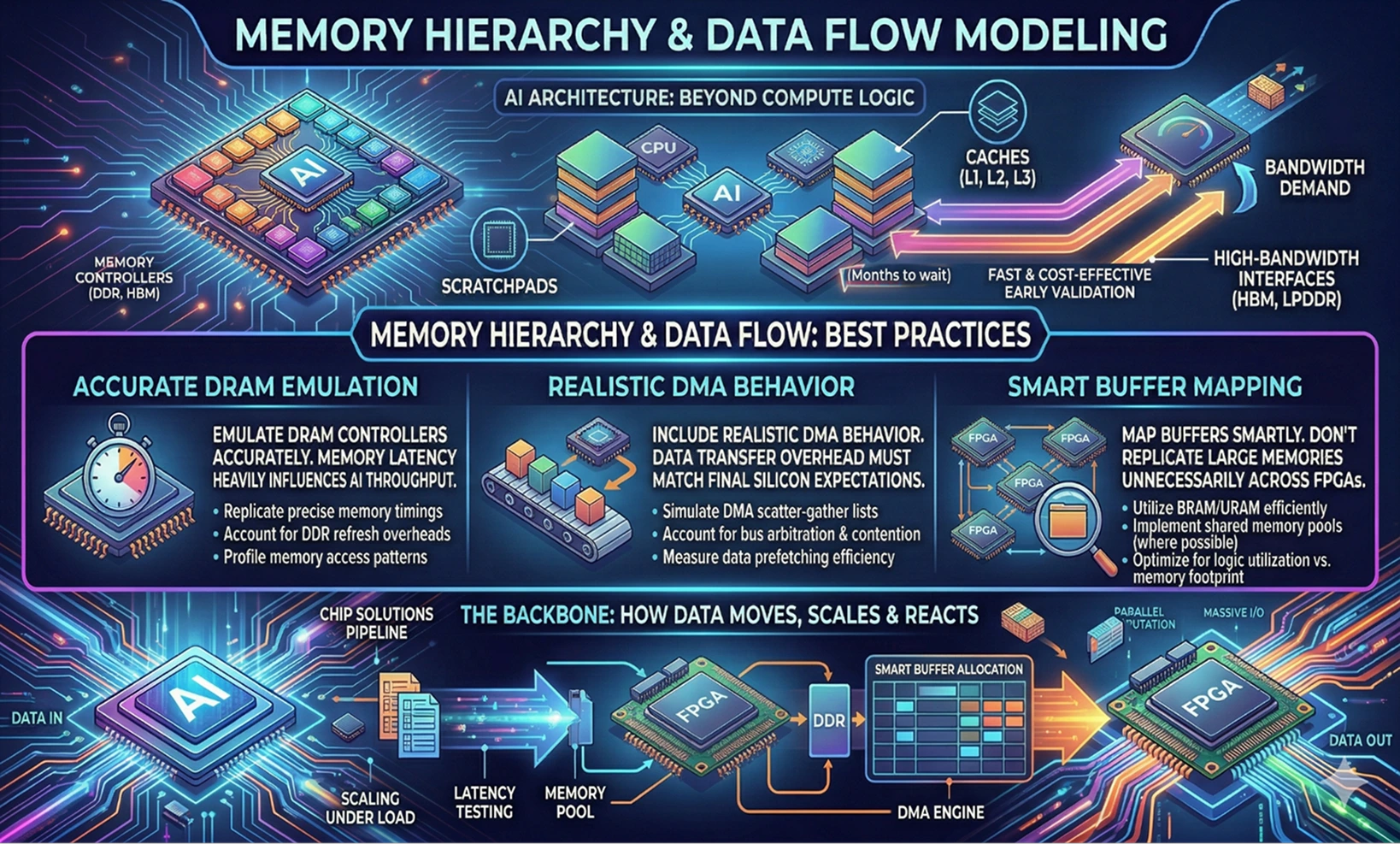
AI architectures thrive on memory bandwidth. Prototyping them means recreating not just the compute logic, but the entire memory hierarchy, including caches, scratchpads, and high-bandwidth interfaces.
Best Practices
- Emulate DRAM controllers accurately. Memory latency heavily influences AI throughput.
- Include realistic DMA behavior. Data transfer overhead must match final silicon expectations.
- Map buffers smartly. Don’t replicate large memories unnecessarily across FPGAs.
Think of this stage as the backbone of your chip solutions pipeline, where you define how data moves, scales, and reacts under load.
Scalable Clocking and Synchronization
Parallelism demands precision timing. In FPGA prototypes, multiple asynchronous clocks can make debugging nearly impossible.
Clocking Strategies That Actually Work
- Define global and local domains. Keep global clocks synchronized, but allow local domains for flexibility.
- Use clock-domain crossing (CDC) verification. It’s boring but absolutely necessary.
- Plan for skew. Even small drifts between boards can cause big issues in large prototypes.
Clock networks in a multi-FPGA setup should mimic the real chip’s architecture, a good practice even before you finalize your custom chip design layout.
Verification and Debugging at Scale
You think debugging a single FPGA is tricky? Try tracing bugs across eight interconnected ones running asynchronous workloads.
Debugging Tips
- Embed logic analyzers and triggers inside the prototype for internal signal observation.
- Use trace compression to handle limited FPGA memory space.
- Automate test benches to re-run scenarios quickly after each tweak.
The goal isn’t perfection; it’s visibility. If you can see where data stalls, deadlocks, or diverges, you’re halfway to solving it.
Hardware-Software Co-Validation
One of the biggest advantages of FPGA prototyping is that it lets hardware and software teams work in parallel. Firmware developers can start testing drivers, schedulers, and memory managers months before final silicon is ready.
Benefits of Co-Validation
- Identify integration bugs early.
- Reduce post-silicon debug time.
- Validate performance tuning in realistic conditions.
This is where your prototype becomes more than just hardware; it becomes a platform for exploring full chip solutions in real-time.
Scaling to the Cloud
With AI models growing larger every year, even physical FPGA clusters might fall short. Cloud-based FPGA environments are filling that gap.
Advantages of Cloud FPGA Prototyping
- Virtually unlimited capacity: Spin up dozens of FPGAs as needed.
- Global collaboration: Teams can access the same hardware setup remotely.
- Scalable experiments: Run multiple AI workloads simultaneously without local infrastructure.
For teams managing geographically distributed chip design projects, this approach speeds up development and reduces capital costs.
From SoCs to Multi‑Die Architectures: A Practical Guide to 3D IC Design
Tessolve: Accelerating AI SoC Innovation with Proven Prototyping Expertise
At Tessolve, we specialize in turning complex ideas into silicon-ready reality. Our hardware engineering teams deliver complete chip design and custom chip design services, from architecture definition to FPGA-based validation. With deep experience in system-level integration, our engineers create scalable chip solutions that handle the toughest AI and high-performance workloads.
Tessolve’s prototyping labs are equipped for large multi-FPGA systems, high-speed validation, and embedded software co-development. By combining design, verification, and test capabilities under one roof, we ensure faster iteration cycles, reduced time-to-market, and optimized performance.
When you’re building tomorrow’s AI hardware, Tessolve gives your ideas the power, precision, and scalability they deserve.
Frequently Asked Questions
1. Why use FPGA prototyping for AI SoC development?
It enables faster validation, parallel testing, and early software integration before expensive silicon tape-out.
2. What challenges occur in multi-FPGA prototyping?
Timing closure, bandwidth bottlenecks, synchronization issues, and resource balancing across multiple interconnected boards.
3. How does FPGA prototyping improve chip design efficiency?
It uncovers functional issues early, reduces re-spins, and accelerates the overall chip design process.
4. Can Tessolve help with scalable FPGA prototyping?
Yes, Tessolve provides advanced chip solutions and FPGA prototyping expertise for complex, high-performance SoC designs.