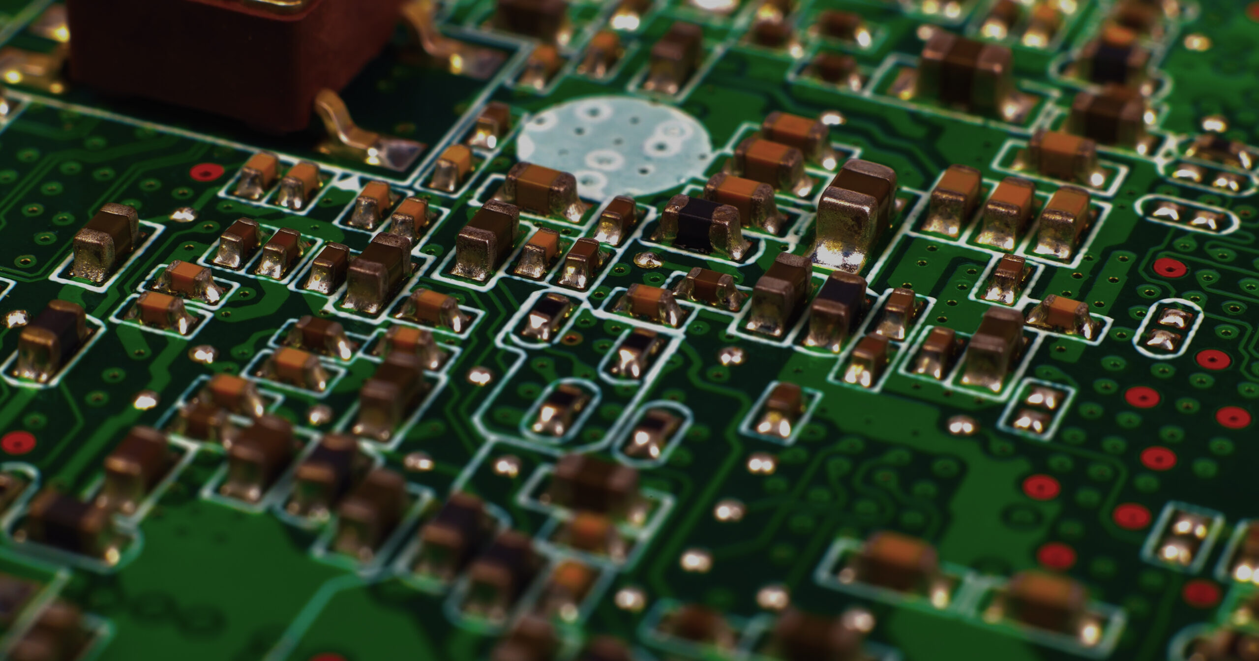
As electronic systems continue to shrink in size while expanding in capability, ultra-fine pitch components have become central to advanced hardware platforms. These components enable greater integration, higher performance, and compact system architecture. However, as pitch dimensions reduce, PCB design complexity increases dramatically. Engineering teams must now manage tighter tolerances, higher routing density, advanced signal constraints, and stricter manufacturing requirements.
Ultra-fine pitch assembly and routing are no longer incremental extensions of conventional PCB layout practices. They introduce a series of interconnected technical challenges that must be addressed systematically from schematic planning through final validation within a structured PCB design service framework.
Core Challenges in Ultra-Fine Pitch PCB Design
Designing PCBs with ultra-fine pitch components demands a structured engineering approach supported by an advanced PCB layout service. The reduced spacing between pins and high-speed performance requirements create multi-layered design pressures.
Let’s understand the primary technical challenges that arise in ultra-fine pitch PCB assembly and routing, and see why they must be managed proactively during development.
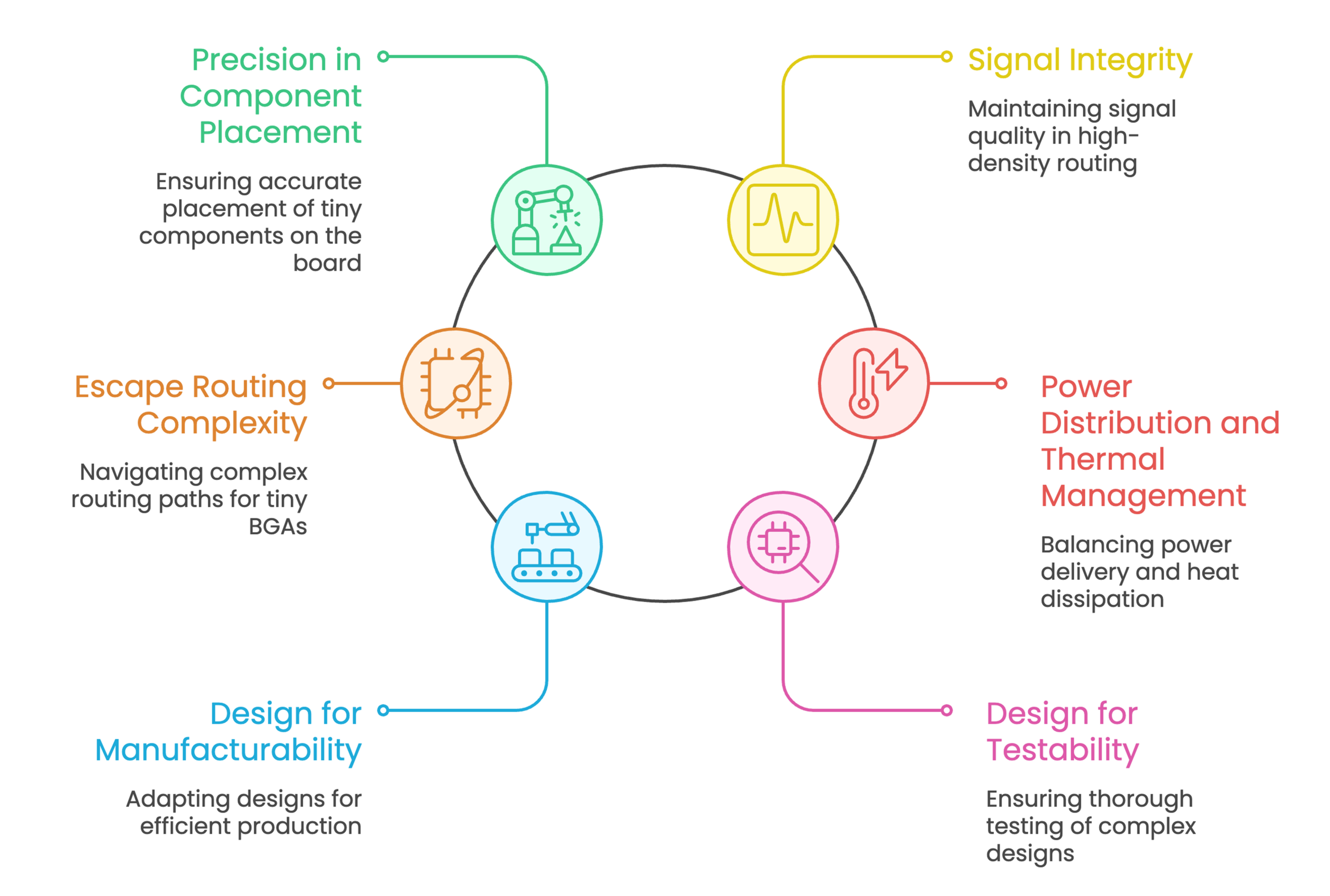
1. Precision in Component Placement and Pad Definition
As pitch sizes shrink, assembly tolerances become significantly tighter. Even minor deviations in pad geometry, solder mask alignment, or placement accuracy can result in bridging, opens, or long-term reliability issues.
In ultra-fine pitch layouts, pad design is no longer a simple footprint exercise. It becomes a manufacturing-critical parameter that directly influences yield and reliability.
Key engineering concerns include:
- Accurate land pattern development aligned with package specifications
- Solder mask design optimisation to prevent bridging
- Controlled pad geometry that supports consistent solder joint formation
- Fabrication-aligned clearances based on manufacturer capabilities
- Strict registration tolerance management
Without disciplined footprint validation and manufacturing alignment, assembly defects can escalate quickly in high-density designs.
2. Signal Integrity in High-Density Routing
Ultra-fine pitch components often support high-speed interfaces, high-bandwidth memory connections, and dense communication protocols. Routing signals within extremely constrained spaces while preserving electrical performance is one of the most demanding aspects of design.
Reduced trace spacing increases the risk of crosstalk and impedance discontinuities. At the same time, limited escape routing channels require innovative routing strategies and stack-up optimisation.
Engineering challenges in this domain include:
- Managing tight trace-to-trace spacing without excessive coupling
- Maintaining impedance control across complex layer transitions
- Controlling return paths in densely packed layouts
- Planning stack-ups that support both routing density and signal performance
- Balancing layer count against manufacturability and cost
Signal integrity must be embedded into the routing strategy from the earliest layout phase. Reactive corrections late in the cycle often lead to design iterations and schedule delays.
3. Escape Routing Complexity in Ultra-Fine Pitch BGAs
Escaping signals from high-density Ball Grid Array packages is one of the most technically intricate tasks in PCB layout. As pitch decreases, the available routing channels between pads reduce significantly, limiting traditional fan-out techniques.
Designers must carefully evaluate via strategies, microvia feasibility, and layer utilisation to ensure all signals can be successfully routed without violating fabrication constraints.
Critical routing considerations include:
- Optimising via placement to maximise channel availability
- Assessing microvia stack and stagger configurations
- Managing via aspect ratios within fabrication limits
- Distributing routing density evenly across layers
- Coordinating stack-up architecture with routing strategy
Improper escape planning can force excessive layer additions, increase cost, and reduce manufacturability margins.
4. Power Distribution and Thermal Management Constraints
High-density components frequently concentrate power consumption within compact areas. Ultra-fine pitch designs often integrate processors, memory devices, and high-speed interfaces that demand stable power delivery and effective heat dissipation.
Poor power distribution network planning can introduce voltage instability, noise coupling, and long-term reliability concerns.
Key power and thermal challenges include:
- Strategic power plane allocation within limited layer budgets
- Decoupling capacitor placement in constrained board regions
- Managing current return paths to reduce loop inductance
- Designing stack-ups that assist thermal spreading
- Preventing localised hot spots near high-density packages
These concerns must be integrated early in the PCB design phase, as late-stage thermal or power corrections can require significant layout rework.
5. Design for Manufacturability Constraints
As pitch dimensions decrease, fabrication tolerances become increasingly critical. Trace width, spacing limits, solder mask alignment, and via registration accuracy must align precisely with manufacturing capabilities.
Small deviations that might be acceptable in conventional layouts can become yield-limiting factors in ultra-fine pitch boards.
Manufacturability challenges include:
- Maintaining minimum trace width and spacing thresholds
- Controlling via aspect ratios within reliable fabrication limits
- Managing layer-to-layer registration tolerances
- Ensuring solder mask alignment precision
- Preventing annular ring reduction during drilling
Design for Manufacturability must be integrated throughout the layout cycle rather than applied as a final review step.
6. Design for Testability and Validation Limitations
High-density layouts restrict physical access to signals for probing and validation. As pad sizes shrink and routing channels narrow, allocating test points becomes increasingly difficult.
Limited test accessibility can complicate debugging and post-production validation if not addressed during design.
Key validation challenges include:
- Early planning of test point placement
- Balancing routing efficiency with signal accessibility
- Integrating functional validation strategies within dense layouts
- Maintaining accessibility without increasing board size
- Coordinating validation strategy with manufacturing test processes
Without proactive Design for Testability planning, engineering teams may face extended bring-up cycles and increased development risk.
Designing for Size and Space Constraints in IoT PCBs: Challenges and Solutions
Tessolve’s Approach to Advanced PCB Engineering
Ultra-fine pitch PCB development requires a structured, system-level engineering approach that integrates schematic architecture, stack-up planning, routing precision, and manufacturability alignment from the outset. At Tessolve, we deliver integrated PCB design service and PCB layout service workflows aligned with semiconductor requirements, impedance control targets, and fabrication tolerances.
Our methodology emphasises early HDI feasibility analysis, signal integrity-driven routing, disciplined Design for manufacturability integration, and validation-aware layout execution. By combining schematic expertise with high-density layout capability, Tessolve provides a complete PCB solution that improves yield, reduces risk, and enables a reliable transition from prototype to production.
Frequently Asked Questions
1. Why are ultra-fine pitch components difficult to assemble on PCBs?
Ultra-fine pitch components have reduced spacing between pins, which increases sensitivity to placement accuracy, pad geometry deviations, and solder mask alignment. Even minor inconsistencies can cause bridging or open connections, making precision and manufacturability alignment critical.
2. How does routing complexity increase with smaller pitch sizes?
Smaller pitch sizes reduce the available routing channels between pads. This limits traditional escape strategies and often requires advanced via structures, microvias, and carefully engineered stack-ups to ensure complete and reliable signal routing.
3. Why is signal integrity a major concern in ultra-fine pitch designs?
High-density components frequently support high-speed interfaces. Tight trace spacing and dense routing increase the risk of crosstalk and impedance discontinuities. Controlled stack-up planning and disciplined routing are necessary to preserve electrical performance.
4. What role does Design for Manufacturability play in high-density PCBs?
As tolerances shrink, fabrication limits become more critical. Integrating Design for Manufacturability throughout the PCB layout service process ensures trace widths, spacing, via structures, and solder mask parameters align with production capabilities, improving yield.
5. How does Tessolve support ultra-fine pitch PCB development?
Tessolve provides an integrated PCB design service and PCB layout service that addresses high-density routing, stack-up optimization, signal integrity, manufacturability alignment, and system-level validation. This structured approach enables reliable, production-ready ultra-fine pitch PCB solutions.


