High-speed SerDes isn’t just another incremental step in electronics; it’s a leap. As interfaces like PCIe Gen5/6, USB4, 112G/224G Ethernet, and advanced AI hardware push data rates to staggering levels, traditional PCB approaches start breaking down. Designs that once worked perfectly now struggle with attenuation, jitter, crosstalk, and thermal instability. That’s why engineers today are turning toward new PCB materials and next-generation routing strategies, rather than relying on legacy practices that can’t support these extreme signal speeds.
If you’ve ever wondered why conventional boards fail under such demanding environments, here are the real reasons high-speed SerDes now require advanced PCB materials and highly disciplined routing techniques.
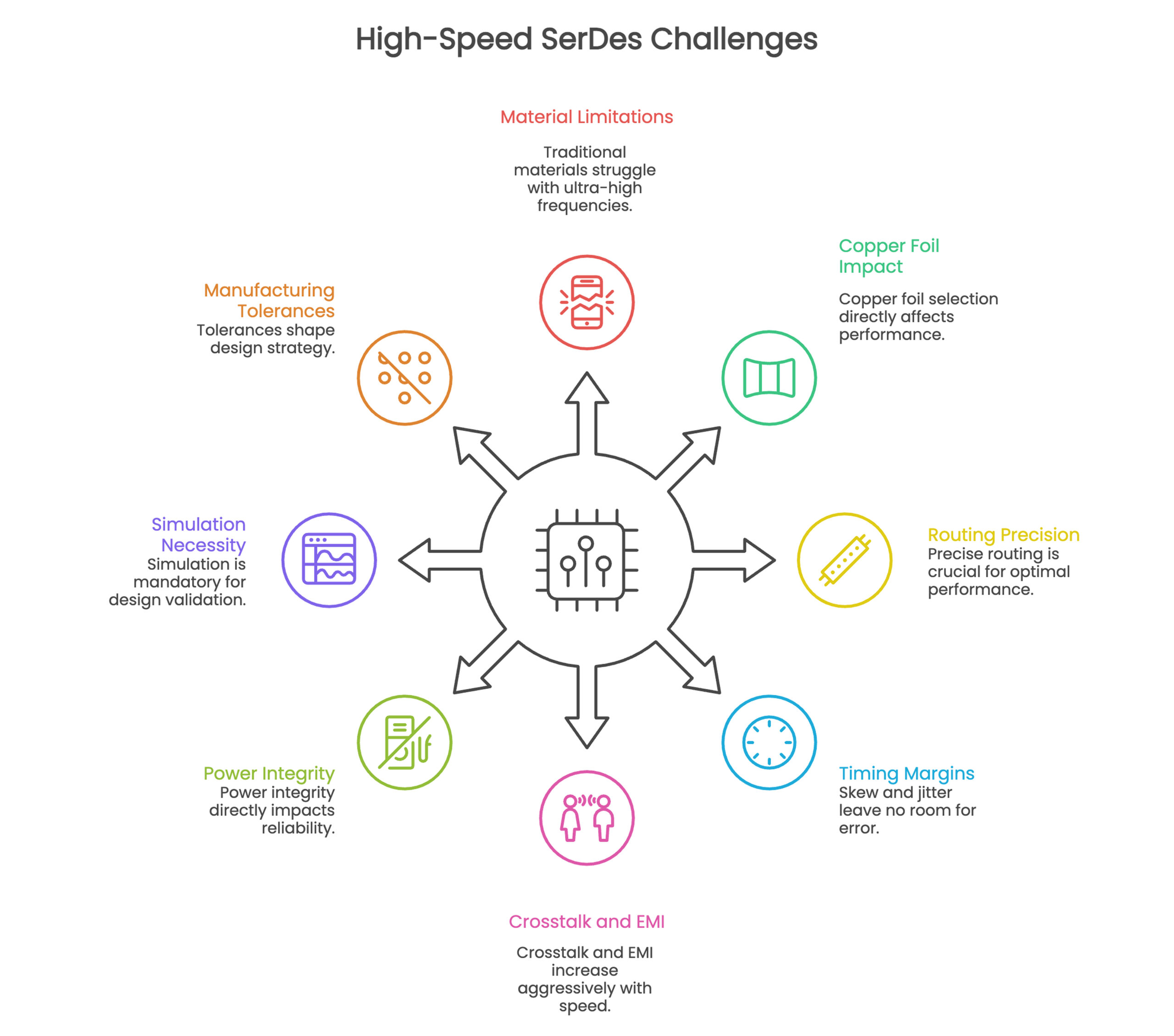
Challenges Driving New PCB Materials & Routing Approaches
Before engineers jump into design decisions, it’s important to understand the real-world hurdles that make traditional boards insufficient:
- Severe signal attenuation and dielectric losses at multi-gigahertz frequencies reduce eye openings and reliability.
- Stringent impedance control and timing budgets leave no tolerance for routing inconsistency or stackup variation.
- Crosstalk, EMI, and noise coupling intensify as channel density and edge rates increase.
- Thermal stability and mechanical reliability become critical with dense, high-power architectures.
- Manufacturing tolerances and material behavior significantly influence performance, demanding smarter material selection and engineering discipline.
Key Reasons Why High-Speed SerDes Requires New PCB Materials and Routing Strategies
1. Traditional PCB Materials Can’t Support Ultra-High Frequencies
Standard FR-4 wasn’t designed for 30–100+ GHz environments. As frequencies rise, dielectric loss increases dramatically, weakening the signal long before it reaches the receiver. Variations in dielectric constant distort impedance, shrink eye diagrams, and introduce bit errors.
Modern designs require low-loss laminates like Rogers, Megtron, or Nelco because they offer stable Dk/Df characteristics, maintain cleaner transmission, and preserve signal integrity across longer channels. Many engineers also use hybrid stackups to balance cost and performance, placing premium material only on layers carrying critical SerDes lanes. This material shift is one key reason organizations increasingly engage specialized PCB design service expertise to get it right the first time.
2. Copper Foil Selection Directly Impacts High-Speed SerDes Performance
While low-loss dielectric materials receive significant attention, copper foil plays an equally critical role in high-speed SerDes design. At multi-gigahertz frequencies, the skin effect confines current to a very thin region near the conductor surface. As data rates reach 25G, 56G, 112G, and beyond, conductor loss becomes a major contributor to total channel loss.
Standard electrodeposited (ED) copper typically has a rough surface profile to enhance adhesion. At high frequencies, this roughness forces current to follow microscopic peaks and valleys, increasing resistance and insertion loss while reducing eye margins.
In thin high-speed stackups, the impact is even greater. Rough copper can:
- Increase conductor loss
- Shift effective Dk and impedance
- Affect capacitance and phase response
To mitigate these effects, advanced designs increasingly specify smoother copper options such as Low Profile (LP), Very Low Profile (VLP), Reverse Treated Foil (RTF), Drum Side Treated Foil (DSTF), or rolled copper for ultra-high-frequency applications.
In modern SerDes systems, copper foil selection is no longer a fabrication detail; it is a deliberate engineering choice that directly influences channel performance and reliability.
3. Routing Precision Now Defines Performance
At ultra-high speeds, traces behave like RF transmission lines rather than simple copper paths. Every bend, via, and stub matters. Maintaining strict impedance control, usually 50Ω single-ended and 100Ω differential, is essential to avoid reflections and degraded eye openings.
This requires:
- Highly accurate stackup engineering
- Consistent trace widths and spacing
- Tight return path management
- Strong correlation between simulation and fabrication reality
Routing is now a carefully engineered discipline, not just a layout task. Poor routing destroys signal integrity even on the best materials.
4. Skew, Jitter, and Timing Margins Leave No Room for Error
SerDes systems rely on differential pairs arriving in sync. Even slight length mismatches introduce skew. Couple that with jitter, and timing margins collapse fast. Designers must ensure:
- Tight length matching
- Strong pair coupling consistency
- Minimal unnecessary serpentine patterns
When timing budgets live in the realm of picoseconds, “close enough” isn’t good enough. This is where working with teams experienced in high-speed PCB solution development becomes essential to ensure stability and compliance.
5. Crosstalk and EMI Increase Aggressively with Speed
As edge rates sharpen, electromagnetic fields expand and interact more aggressively with nearby signals. Dense layouts make this worse. Without careful planning, SerDes lanes radiate energy into each other, causing unpredictable system failures.
Modern routing practices demand:
- Greater spacing between differential lanes
- Layer-to-layer routing orthogonality
- Ground referencing and shielding
- Strategic via stitching
Engineers now treat EMI and crosstalk as primary design constraints, not afterthoughts, which is why experienced PCB hardware design capability matters tremendously.
6. Power Integrity Directly Impacts SerDes Reliability
Power integrity isn’t just about supply; it now directly shapes signal quality. Poor PDN design injects noise into SerDes, causing timing instability and channel degradation. Clean, stable power rails are critical at these speeds.
This requires:
- Robust PDN architecture
- Thoughtful decoupling strategies
- Low-impedance plane design
- Early-stage PI simulation
Power integrity and signal integrity are now inseparable engineering priorities.
7. Simulation Is Now Mandatory, Not Optional
Guessing no longer works in a SerDes world. Before fabrication, engineers must validate behavior using advanced SI/PI simulation tools to predict loss, analyze eye performance, evaluate jitter, and confirm compliance.
Simulation-driven design reduces iterations, prevents expensive respins, and accelerates development. Many companies lean on expert PCB design service partners who integrate simulation into every development phase, ensuring reliability before boards ever hit the fab.
8. Manufacturing Tolerances Now Shape Design Strategy
High-speed boards require tighter tolerances, advanced stackups, precise dielectric control, reliable via structures, and thermally stable materials. Even slight fabrication deviations can impact performance, meaning design and manufacturing collaboration must now be deeply aligned.
This is why organizations increasingly engage engineering partners with end-to-end PCB solution capabilities and strong PCB hardware design experience, to ensure designs are not only high-performance on paper, but manufacturable and reliable in real-world production.
Channel Modeling and Simulation for High-Speed PCB Design Verification
Tessolve: Empowering the Future of High-Speed PCB Design
At Tessolve, we understand what it takes to engineer reliable, high-speed systems in today’s rapidly evolving electronics landscape. With deep expertise in high-speed SerDes design, advanced stackup engineering, controlled impedance routing, SI/PI simulation, validation, and end-to-end hardware execution, we help global customers build performance-driven boards with confidence. Our Tessolve teams combine engineering excellence with strong lab infrastructure, compliance knowledge, and manufacturing alignment to deliver designs that perform, scale, and succeed in real-world deployment. Whether you’re pushing data rates higher, simplifying complexity, or accelerating development cycles, Tessolve stands as your trusted partner for robust, future-ready PCB innovation.
Frequently Asked Questions
1. What is SerDes, and why is it important for high-speed PCB design?
SerDes (Serializer/Deserializer) converts parallel data to serial streams, enabling ultra-high-speed communication with minimal signal loss.
2. Why do traditional FR-4 materials fail in high-speed SerDes applications?
FR-4 has high dielectric loss and variable Dk at gigahertz frequencies, causing signal attenuation and integrity issues.
3. How does routing impact SerDes signal integrity on PCBs?
Trace width, spacing, impedance control, and differential pair management all affect reflections, crosstalk, and overall signal reliability.
4. What role does simulation play in high-speed PCB design?
SI/PI simulation predicts signal loss, jitter, and eye closure, preventing costly board respins and improving first-pass success.
5. Why are new PCB materials necessary for high-speed SerDes designs?
Low-loss laminates ensure stable impedance, reduce signal attenuation, and maintain signal integrity at very high data rates.


