
The path from Register Transfer Level (RTL) design to a final GDSII layout is the heart of semiconductor development. This pre-silicon flow has traditionally been a highly iterative and time-consuming process involving complex steps like synthesis, verification, place-and-route, and signoff, all prone to late-stage surprises.
With the rise of Artificial Intelligence (AI) and Machine Learning (ML), the entire RTL-to-GDS flow is undergoing a fundamental transformation. AI/ML is effectively utilized as a predictive and optimization layer, enhancing existing Electronic Design Automation (EDA) tools. By embedding predictive models and intelligent optimization directly into the flow, companies are achieving unprecedented gains in speed, quality, and Power, Performance, and Area (PPA).
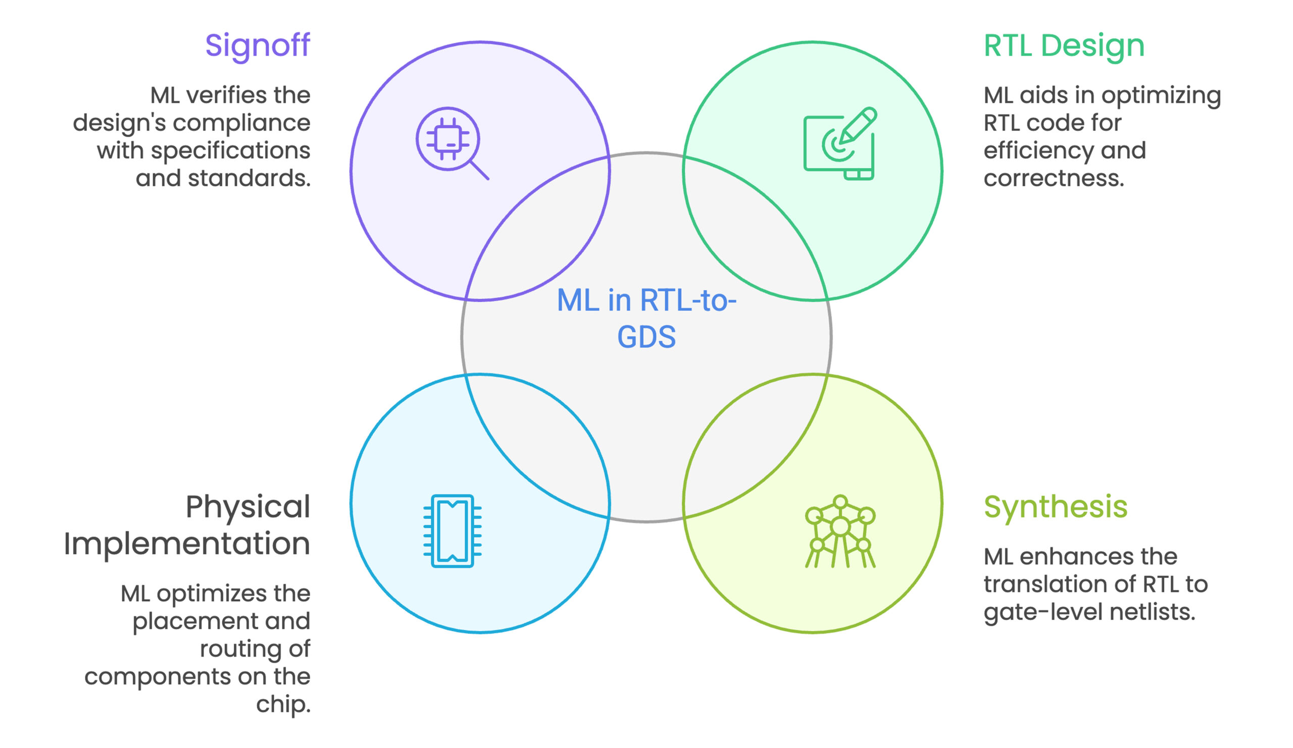
Effective Utilization of ML Across the RTL-to-GDS Flow
AI/ML does not replace existing tools; it integrates predictive intelligence to solve traditionally complex, iterative, or manual challenges at each stage, ensuring smoother handoffs and minimizing expensive late-stage rework.
1. RTL Design & Functional Verification Stage (Early Closure)
This is the earliest stage where functional and logic errors are introduced, which are exponentially more expensive to fix later.
- Smart RTL Linting and Bug Prediction: ML models trained on historical bug reports and code patterns detect issues and predict where functional errors, non-synthesizable code, or clock/reset issues are most likely to exist. The key benefit is Early Defect Elimination, catching bugs during coding and preventing costly functional escapes that only surface in gate-level or post-layout simulation.
- Regression Prioritization and Adaptive Testing: ML ranks the most failure-prone test cases and intelligently selects a minimal, high-impact regression suite based on recent code changes. This results in Faster Feedback Loops by drastically reducing regression runtimes and accelerating the verification cycle.
- Constraint Definition Assistants: ML automatically validates and refines design constraints (e.g., timing, power) against design intent and historical data. This offers the benefit of Reduced Setup Time and Errors, ensuring high-quality, achievable PPA targets from the start.
2. Synthesis & Physical Implementation Stage (PPA Optimization)
This stage translates RTL logic into physical gates and places them on the chip, determining the final PPA.
- PPA Prediction and Synthesis Optimization: ML models predict the power, performance, and area impact of synthesis options before running full synthesis, guiding the tool toward the optimal settings. The benefit is Accelerated PPA Closure, finding the optimal trade-off point faster and minimizing the number of synthesis-to-place-and-route (P&R) iterations.
- Placement and Routing Surrogate Modeling: ML models predict the likelihood of routing congestion, timing violations, and IR drop based on early placement data. This enables a higher-quality initial P&R by guiding better placement and floorplan seeds upfront, minimizing late-stage post-layout fixes.
- Timing Closure Acceleration: ML analyzes timing reports and suggests the most effective physical cells or techniques to resolve specific timing paths. This drastically reduces the iterations needed, automating and optimizing a highly difficult part of physical design.
3. Signoff Stage (First-Silicon Success)
The final stage ensures the design is manufacturable and meets all requirements.
- Signoff Failure Prediction (DRC/LVS/Timing): ML models predict the likelihood of DRC (Design Rule Check), LVS, and timing signoff failures based on intermediate physical data. The core benefit is Higher First-Silicon Success, allowing teams to proactively resolve manufacturability issues, avoiding costly chip respins and project delays.
- Yield Prediction and Hotspot Detection: Models correlate final layout data with historical silicon yield data to flag potential weak areas or yield-limiting hotspots. This directly leads to Improved Silicon Yield by guiding minor layout adjustments to maximize the number of working chips produced per wafer.
Important Note on AI/ML-Assisted Signoff
While AI/ML tools significantly accelerate decision-making across the RTL-to-GDS flow, final signoff must always be performed by experienced design engineers. AI-ML outputs should be treated as decision-support insights, not autonomous approvals. All critical signoff activities such as timing, DRC/LVS, power, and manufacturability require human validation to ensure design intent, compliance, and risk mitigation. This human-in-the-loop approach ensures reliability, accountability, and first-silicon success while still benefiting from AI-driven speed and optimization.
Key Advantages: Gains at Each Stage
The benefits of AI/ML are clearly articulated by the time-to-market reduction and quality improvement at every step:
- Accelerated Design Closure: Predictive modeling (Surrogate Modeling) eliminates the “blind trial-and-error” approach in P&R and synthesis, cutting down manual effort and tool runtime.
- Higher First-Silicon Success: Early error detection, especially in RTL and signoff prediction, minimizes costly respins.
- Enhanced Engineer Productivity: AI takes over repetitive tuning tasks (like constraint optimization and test selection), allowing expert engineers to focus on high-value, complex innovation.
- Tighter Collaboration: By providing early visibility, e.g., flagging a high-risk RTL module or predicting congestion, AI aligns cross-functional teams, minimizing friction and rework across silos.
- Knowledge Preservation and Scalability: ML models effectively encode design patterns and historical lessons learned, making teams more effective and adapting to growing SoC complexity across technology nodes.
Practical AI Patterns in Use Today
Chip teams are already adopting AI in practical, incremental ways. Some proven patterns include:
- Data-driven verification – Collecting test results, RTL changes, and bug logs to train models that predict likely failures.
- Surrogate P&R modeling – Using ML to approximate placement congestion and timing, guiding placement seeds for better initial results.
- Constraint generation assistants – Automatically refining timing and synthesis constraints to reduce manual tuning errors.
- Adaptive regression – Continuously improving test selection models with new failure data.
Rather than replacing engineers, these AI tools act as intelligent assistants, making expert teams more efficient and effective.
Challenges in Adopting AI Workflows
Adoption, however, requires overcoming some hurdles:
- Data readiness – Teams need well-structured historical data to train effective models.
- Trust in predictions – Engineers must see clear reasoning behind AI recommendations.
- Seamless tool integration – APIs and EDA plug-ins are essential for smooth adoption.
- Cross-team alignment – ML workflows must complement, not disrupt, established ownership and responsibilities.
When approached step by step, these challenges become manageable, and the return on investment quickly becomes evident.
The Road Ahead for AI in Chip Design
Looking forward, the industry is moving toward:
- Pre-trained AI models embedded in EDA tools.
- Larger datasets shared across ecosystems (with anonymization).
- Domain-specific large language models (LLMs) trained on RTL, logs, and constraints.
- Natural language interfaces for debugging and verification.
As these advancements mature, chip design companies that embrace AI-driven flows will enjoy a clear competitive advantage in both speed and quality.
RTL Design for AI Workloads: Power Efficiency and Data Movement in Focus
Tessolve: Your Partner in AI-Enabled RTL-to-GDS
At Tessolve, we recognize the critical role AI and ML now play in accelerating RTL design to tapeout. As a full-stack semiconductor engineering partner, we provide end-to-end VLSI and ASIC services, from RTL coding and functional verification to physical design, timing signoff, and GDSII delivery. Our global test labs, product engineering capabilities, and strong ecosystem partnerships ensure a complete silicon lifecycle solution.
What sets us apart is our commitment to innovation, leveraging ML-driven verification, automated optimization, and data-backed workflows to reduce design cycles and minimize risks. For customers seeking reliable, AI-augmented RTL-to-GDS execution combined with robust post-silicon validation, Tessolve offers unmatched expertise. With our proven track record and advanced engineering capabilities, we help clients bring products to market faster, smarter, and with greater confidence.
Disclaimer
To sign off on the output of any AI/ML-assisted tool, it is essential to thoroughly review all inputs and ensure that they are 100% golden. AI-driven recommendations are only as reliable as the quality, accuracy, and completeness of the input data provided. Therefore, final validation, engineering review, and signoff must always be performed by qualified design experts to guarantee correctness, compliance, and tapeout readiness.