In the rapidly evolving Internet of Things (IoT) era, the proliferation of interconnected devices has led to an unprecedented demand for efficient and reliable hardware solutions. At the heart of these devices lies the critical component that drives functionality and performance: the microchip. Designing power-efficient chips is paramount to ensure the sustainability and effectiveness of IoT applications.
The Imperative for Power Efficiency in IoT Devices
IoT devices are often deployed in environments where replacing or recharging batteries is challenging. Consequently, minimizing power consumption extends the device’s lifespan and reduces maintenance costs. Moreover, as the number of IoT devices scales into the billions, the cumulative energy consumption becomes a significant concern, both economically and environmentally.
Power efficiency is also crucial for improving device performance. Low-power chips generate less heat, reducing the need for extensive cooling mechanisms. This not only lowers production costs but also allows manufacturers to create compact and lightweight IoT devices, enhancing their appeal and usability.
Strategies for Power-Efficient Chip Design
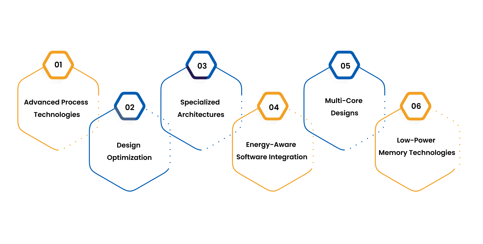
- Advanced Process Technologies: Utilizing cutting-edge fabrication processes, such as FinFET and Gate-All-Around (GAA) transistors, allows for reduced power leakage and lower operating voltages, enhancing overall energy efficiency.
- Design Optimization: Implementing design techniques like clock gating, power gating, and dynamic voltage and frequency scaling (DVFS) enables chips to adjust their power usage based on workload demands, thereby conserving energy during low-activity periods.
- Specialized Architectures: Developing application-specific integrated circuits (ASICs) tailored for particular IoT functions can outperform general-purpose processors in both efficiency and performance, as they are optimized for specific tasks.
- Energy-Aware Software Integration: Collaborating closely with software developers to create energy-efficient algorithms ensures that the software complements the hardware’s power-saving features, leading to holistic system efficiency.
- Multi-Core Designs: Incorporating multiple cores within a chip allows tasks to be distributed efficiently, reducing the workload on individual cores and lowering power consumption.
- Low-Power Memory Technologies: Using memory architectures optimized for low energy consumption, such as SRAM or LPDDR, further enhances the power efficiency of chips.
The Role of VLSI Design Engineering in Power Efficiency
Very Large Scale Integration (VLSI) design engineering plays a pivotal role in the development of power-efficient chips. By integrating millions of transistors into a single chip, VLSI design engineers can implement complex functionalities while optimizing for power consumption. Techniques such as hierarchical design, modular approaches, and the use of low-power libraries are instrumental in achieving energy-efficient outcomes.
Advanced simulation tools used in VLSI circuit design enable engineers to analyze power consumption at various stages of design. These tools facilitate early detection and resolution of power-related issues, ensuring efficient designs from the outset.
Challenges in Power-Efficient Chip Design
Designing power-efficient chips for IoT applications presents several challenges:
- Thermal Management: As devices become more compact, dissipating heat effectively without compromising performance is a significant concern.
- Manufacturing Variability: Ensuring consistent performance across chips despite variations in the manufacturing process requires robust design strategies and thorough testing.
- Security Considerations: Implementing security features that protect against threats without imposing substantial power overhead is crucial for maintaining device integrity.
- Balancing Cost and Efficiency: Achieving power efficiency often requires advanced materials and processes, which can increase production costs. Striking a balance between affordability and performance is a persistent challenge for chip design companies.
Emerging Trends in Power-Efficient Chip Design
The field of chip design is continually evolving, with emerging trends aimed at enhancing power efficiency:
- Chiplet Architectures: Modular chip designs, known as chiplets, allow for the integration of heterogeneous functions, enabling optimized power management and improved performance.
- AI-Driven Design Tools: Artificial intelligence is being leveraged to automate and optimize various aspects of chip design, resulting in more efficient and effective design processes.
- Advanced Materials: Research into materials beyond traditional silicon, such as silicon photonics, promises faster and more energy-efficient chips, potentially revolutionizing the industry.
- Edge Computing Integration: As IoT devices increasingly process data locally, power-efficient chips designed for edge computing are gaining prominence. These chips minimize energy use while delivering high-performance computation.
- 3D ICs: Three-dimensional integrated circuits stack multiple layers of components, enabling compact designs with shorter interconnections, which reduce power consumption.
Tessolve: Pioneering Power-Efficient Chip Design Solutions
At Tessolve, we are at the forefront of delivering comprehensive semiconductor engineering solutions that address the challenges of power-efficient chip design. Our expertise spans the entire spectrum of chip development, from design and verification to testing and validation. By leveraging advanced VLSI circuit design methodologies and collaborating closely with clients, we ensure that the chips we develop meet the stringent power efficiency requirements essential for IoT applications. Our team of seasoned professionals and our state-of-the-art infrastructure enable us to provide end-to-end support, making us a trusted chip design company for organizations worldwide.
Tessolve’s holistic approach integrates hardware and software optimization, ensuring seamless energy efficiency. From prototyping to mass production, we stand by our clients every step of the way, delivering innovative solutions that power the IoT revolution sustainably.
Ensuring First-Pass Success with VLSI Verification Strategies
Let’s Conclude
As the IoT landscape continues to expand, the demand for power-efficient chip design becomes increasingly critical. By embracing advanced technologies, optimizing design methodologies, and staying abreast of emerging trends, chip design companies can develop solutions that meet the power efficiency needs of modern IoT devices. Through the dedicated efforts of VLSI design engineers and the adoption of innovative approaches, the industry is well-positioned to create sustainable and efficient hardware for the interconnected world.
Partnerships with industry leaders like Tessolve will be instrumental in shaping the future of power-efficient VLSI design engineering. By delivering cutting-edge solutions, Tessolve continues to empower businesses to thrive in an increasingly connected and energy-conscious world.
- Integrated Design Tools: Utilize simulation tools that support co-simulation, enabling seamless analysis of SI and PI within the same environment. This integration facilitates a more comprehensive understanding of the interactions between signals and power delivery.
- Accurate Modeling: Ensure that models for components, interconnects, and power delivery networks are accurate and reflect real-world behavior. This accuracy is crucial for reliable simulation results.
- Cross-Disciplinary Collaboration: Encourage collaboration between signal integrity engineers, power integrity specialists, and layout designers. A multidisciplinary approach ensures that all aspects of the design are considered holistically.
- Iterative Validation: Perform simulations at various stages of the design process, from initial concept to final layout. Iterative validation helps in catching issues early and refining the design progressively.
- Design Rule Enforcement: Using SI/PI co-simulation results to refine design rules can lead to systemic improvements across multiple projects, improving overall PCB hardware design workflows.