
Semiconductor technology is progressing at a breathtaking rate, becoming an indispensable component of contemporary life. Behind the focal point of this development are two key factors: design and fabrication. And both driven by the capabilities of VLSI and embedded solutions.
VLSI chip design is all about designing sophisticated semiconductor devices, circuits, and small systems driven by in-built solutions. By integrating millions of MOS transistors onto one chip, VLSI design cycle provides the ability to develop powerful, efficient, and innovative electronic systems.
Want to know more about VLSI Chip? Let’s take a step-by-step look at the VLSI Chip Design and development, see why Tessolve is the go-to partner for making such intricate designs a reality.
About VLSI Design Cycle
VLSI design flow involves integrating millions of transistors into a single chip. A chip design VLSI is used to develop small, high-performance electronic systems used in smartphones, automotive electronics, medical devices, and many more. VLSI chip design system facilitates innovation by integrating sophistication with cost-effectiveness, thereby becoming the backbone of current semiconductor technology.
Understanding The VLSI Design Cycle
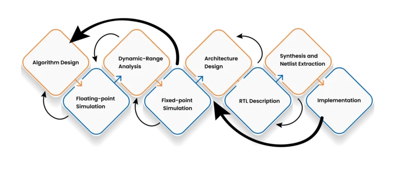
The VLSI design cycle is a process that requires a detailed understanding of various aspects involved in creating integrated circuits. At the design planning stage, the specifications of the chip are defined, and the requirements for power, performance, area, and functionality are established. This stage involves collaboration between hardware and software engineers to ensure the chip’s functional requirements are met.
In the RTL design stage, the functional behavior of the chip is defined using a hardware description language (HDL). This is followed by logic synthesis, where the HDL is converted into a gate-level netlist. The gate-level netlist defines the chip’s logical structure and is used in the subsequent physical design stage.
The physical design stage involves the creation of a layout that defines the chip’s physical structure. This stage includes floor planning, placement, and routing of the chip’s components, and requires expertise in algorithms, data structures, and physical design tools.
Verification is a critical stage in the VLSI chip design cycle, where the chip’s functionality is tested against the specifications defined in the design planning stage. This stage involves simulation, formal verification, and testing, and requires expertise in software engineering and computer science. Now, in the upcoming sections of the blog, we will discuss VLSI chip design and engineering services at Tessolve.
Innovative Approaches in VLSI Chips Memory Management: Design Strategies
Common Challenges in VLSI Design Cycle
Power Consumption: Power consumption is a critical concern in VLSI hardware design, particularly with the growing demand for portable, battery-powered, and energy-efficient devices. As circuits become increasingly complex and the transistor count rises, managing power usage becomes essential to maintain performance while reducing energy costs. Designers employ several strategies to optimize power consumption:
- Power Gating: This technique involves shutting off inactive portions of the circuit to minimize power use during idle periods, significantly reducing leakage power.
- Voltage Scaling: By lowering the supply voltage, dynamic power consumption is reduced. However, voltage scaling must be carefully balanced against performance requirements to maintain reliable circuit operation.
Effective power optimization ensures longer battery life in portable devices and improved energy efficiency in larger VLSI systems.
- Timing Closure: Timing closure is the process of ensuring that all signal paths in a circuit meet the required timing constraints, which is crucial for synchronization between components and overall circuit reliability. Increasing circuit complexity and higher operating frequencies make timing closure a significant challenge. Common techniques used to address these challenges include:
- Pipelining: Dividing the circuit into multiple stages to reduce the critical path delay and increase throughput.
- Retiming: Adjusting the placement of registers to balance path delays and optimize performance.
- Clock Tree Synthesis (CTS): Optimizing the clock distribution network to minimize clock skew and ensure consistent timing across the circuit.
Achieving timing closure is vital to prevent timing violations and guarantee reliable, high-performance operation.
- Physical Design: Physical design focuses on the placement and routing of circuit components on a chip while optimizing performance, power, and area (PPA). It is a pivotal stage in VLSI design process because it directly affects circuit speed and efficiency. A major challenge in physical design is balancing area reduction with performance requirements, shrinking a circuit can lower power consumption but may increase signal delays for a VLSI hardware.
For addressing these challenges, designers leverage advanced placement and routing algorithms that optimize:
- Area utilization to accommodate more functionality in limited space.
- Signal delay minimization for faster and more reliable circuits.
By effectively managing these trade-offs, physical design ensures efficient and high-performing VLSI circuits solution.
- Design for Testability (DFT): Design for Testability (DFT) ensures that integrated circuits can be thoroughly tested for manufacturing defects, guaranteeing product quality and reliability. The primary challenge in DFT is achieving high fault coverage without excessive area overhead. Key DFT techniques include:
- Scan Compression: Reduces the number of test patterns while maintaining high coverage.
- Built-In Self-Test (BIST): Embeds test mechanisms within the circuit to enable autonomous testing.
These methods allow for efficient testing of complex circuits by minimizing test time and data volume while maintaining performance and area efficiency.
- Design Verification: Design verification validates that a circuit functions correctly and meets the specified requirements under all operating conditions. With increasing design complexity, exhaustive testing becomes a challenge. Modern verification methodologies include:
- Constrained Random Testing: Generates a wide range of input scenarios to uncover potential corner-case issues.
- Formal Verification: Mathematically proves that the design adheres to its specifications.
Simulation Acceleration: Speeds up verification cycles using hardware-assisted or optimized simulation techniques. Advanced verification ensures higher coverage, reduces errors, and accelerates the overall design cycle.
Overcoming the Challenges
To successfully address these challenges, VLSI designers rely on specialized tools and techniques across each design stage:
- Power Analysis Tools: Identify and optimize power hotspots throughout the design.
- Timing Analysis Tools: Ensure timing closure by analysing and optimizing critical paths.
- Physical Design Tools: Provide automatic placement and routing for optimal PPA trade-offs.
- DFT Tools: Facilitate test insertion, pattern generation, and fault simulation.
- Verification Tools: Enable functional verification, performance evaluation, and coverage analysis through simulation and formal methods.
By leveraging these tools and methodologies, VLSI designers can efficiently overcome design challenges, ensuring reliable, high-performance, and energy-efficient VLSI circuits.
VLSI Chip Design and Engineering Services At Tessolve
VLSI design goes through multiple stages, from the high-level specification to the final physical implementation of the integrated circuit. Here are the key stages of the VLSI design flow and how Tessolve can help in each stage:
- Requirements and specification: This stage involves defining the system requirements and creating a high-level specification for the VLSI design. Tessolve can assist with defining the requirements and creating a comprehensive specification document that can serve as a reference for the rest of the design process.
- RTL design and verification: In this stage, the RTL (register-transfer level) code is written and verified using simulation and other verification techniques. We can provide experienced RTL designers to create high-quality RTL code and perform verification using industry-standard tools and methodologies.
- Synthesis and Place & Route (P&R): In this stage, the RTL code is synthesized into gate-level netlists and then placed and routed to create the final physical design. We have expertise in using advanced synthesis and P&R tools to produce optimized designs that meet performance and power requirements.
- Physical Verification: In this stage, the final physical design is verified for correctness and to ensure that it meets the design constraints. We can assist with performing physical verification using industry-standard tools and methodologies.
- Tapeout: The final physical design is sent to the foundry for fabrication at this stage. We can assist with preparing the final design files and coordinating the tapeout process with the foundry.
- Silicon validation and debug: In this stage, the fabricated chips are tested to validate the design and debug any issues that may have arisen during fabrication. We can support silicon validation and debugging by providing experienced engineers with expertise in silicon bring-up and debugging.

Conclusion
In conclusion, the VLSI chip design cycle is crucial in designing and developing integrated circuits. It involves various stages such as requirement gathering, system-level design, RTL (register-transfer level) design, functional verification, synthesis, place and route, and physical verification. The VLSI design cycle helps ensure integrated circuits’ correct functioning and helps identify and resolve design issues before the manufacturing stage.
Choosing the best VLSI company is crucial for the proper implementation of the VLSI design cycle for the success of any integrated circuit project. It is critical in ensuring high-quality, reliable, and cost-effective end products.
Tessolve (VLSI company) is a leading semiconductor engineering and technology solutions provider with a team of highly skilled engineers and a commitment to innovation. We are dedicated to helping companies in the industry overcome complex technical challenges such as VLSI solutions.
Download Brochure
VLSI Design
Accelerate your VLSI journey with Tessolve’s VLSI chip designs and engineering services.
Brochure PDF Download
Get in Touch
Connect with us at Tessolve, your trusted semiconductor engineering and technology solutions. With a team of experts specializing in VLSI design and integration technologies, we have successfully completed over 100 projects, delivering high-performance transistors on chips globally. Contact us to optimize your next big idea and start your innovation journey today.
Impact of AI on VLSI Design
FAQ
1. Why is the VLSI design cycle important?
It ensures that integrated circuits function correctly, meet performance standards, and are manufacturable, reducing risks and development costs.
2. What are the main applications of VLSI chip design Process?
VLSI is used in smartphones, computers, automotive electronics, and many consumer and industrial devices requiring compact, high-performance chips.
3. What tools are commonly used in VLSI circuit design?
Electronic Design Automation (EDA) tools are used for synthesis, placement, routing, and verification to automate and optimize the design process. Learn about How AI-Powered EDA Tools Shape the Future of Chip Design.