In the fast-paced world of semiconductor design, the demand for innovative and efficient solutions is ever-growing. One effective approach to meet this demand is leveraging Semiconductor IP (Intellectual Property) design through pre-designed blocks. In today’s landscape, nearly 90% of a modern SoC is comprised of third-party or internal IP, allowing engineers to focus on the “secret sauce” that differentiates their product. These functional components offer a range of benefits that streamline the design process and drive product development.
Understanding Semiconductor IP Design
Semiconductor IP (Intellectual Property) design refers to creating reusable building blocks or components for semiconductor chips. It involves designing and developing functional modules, such as processors, memory, or communication interfaces, which can be integrated into larger chip designs.
Understanding semiconductor IP design requires knowledge of digital and analog circuit design, computer architecture, and system-level considerations. Designing semiconductor IP involves various stages, including specification, architecture, design, verification, and documentation. In 2026, “Shift-Left” verification has become the industry standard, where IP blocks are validated using AI-driven Digital Twins, software models of the hardware, months before the physical silicon is even manufactured. Considering the target application and manufacturing process, IP designers must optimize for power, performance, area, and reliability.
Semiconductor IP plays a crucial role in the semiconductor industry by enabling faster and more efficient chip development. It allows chip designers to focus on specific functionalities, reduce time-to-market, and leverage proven designs. Understanding semiconductor IP design is essential for engineers and companies aiming to create innovative and competitive semiconductor solutions in today’s rapidly evolving technological landscape.
Types of Pre-Designed Blocks
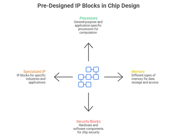
Various types of pre-designed blocks are available for integration into semiconductor chip designs. Some common types include:
- Processors: Pre-designed processor IP blocks are widely used in chip design. These include general-purpose processors (ARM or MIPS cores) and application-specific processors (digital signal processors or graphics processing units).
- Memory: Pre-designed memory IP blocks offer different types of memory, such as SRAM (Static Random-Access Memory), DRAM (Dynamic Random-Access Memory), Flash memory, or cache memory. Beyond standard RAM, High Bandwidth Memory (HBM3e/4) IP is now essential for AI data centers, often integrated closer to logic chiplets in 3D stacks. Memory blocks are essential for storing and accessing data in the chip.
- Security Blocks: With the increasing importance of cybersecurity, pre-designed security IP blocks are available to enhance chip security. Hardware “Root of Trust” (RoT) and Quantum-Safe Cryptographic engines are now mandatory for protecting IoT and automotive data against future quantum threats. These blocks may include cryptographic engines, secure boot modules, tamper-resistant elements, and other security-related components.
- Specialized IP: Various specialized IP blocks cater to specific industries or applications. For example, in automotive designs, IP blocks exist for advanced driver-assistance systems (ADAS), vehicle networking, or infotainment systems.
The Future of Modular Silicon: The Chiplet Revolution
The semiconductor industry is moving beyond traditional “monolithic” SoC designs toward a modular “Chiplet” architecture. This shift allows engineers to break a single large chip into smaller, functional dies (chiplets) that can be manufactured on different process nodes, for example, pairing a cutting-edge 2nm CPU chiplet with a cost-effective 6nm I/O chiplet in the same package. This “Heterogeneous Integration” is primarily driven by the UCIe (Universal Chiplet Interconnect Express) standard, which enables IP blocks from different vendors to communicate seamlessly. By leveraging chiplets, companies can drastically improve manufacturing yields, reduce development costs, and create highly customized AI accelerators without the risk of a full-scale silicon redesign.
Decoding VLSI CAD: Exploring Design, Flow Algorithms, and Tools
Wrapping Up
After going through the above blog, we believe you are now quite aware of the semiconductor IP design, its type, and the implementation of Pre-designed blocks. Moreover, the functions of a semiconductor IP design depend on choosing the best semiconductor engineering services in India.
Unlock the power of semiconductor innovation with Tessolve, your trusted semiconductor design company. We specialize in IP “Hardening”, the process of optimizing soft IP for specific 3nm or 2nm manufacturing nodes to ensure guaranteed power and speed targets. We bring extensive design, verification, validation, and testing expertise to help you create cutting-edge semiconductor solutions. Whether you need assistance with RISC-V customization, Chiplet integration via UCIe standards, or test program development, our experts guide you at every step.
With our industry-leading services and deep understanding of the semiconductor landscape, we can accelerate your product development, enhance performance, and ensure reliability. Contact Tessolve today, and let us collaborate to bring your semiconductor designs to life. Together, we’ll shape the future of technology.
Frequently Asked Questions
1. What is an IP in the semiconductor industry?
Semiconductor IP is a reusable, pre-designed unit of logic or chip layout used as a building block for integrated circuits.
2. What IP blocks improve AI inference performance?
Neural Processing Units (NPUs), Tensor Processing Units (TPUs), and optimized GPU cores accelerate parallel computations for real-time AI decision-making.
3. How can ready-to-use IP blocks speed up chip development?
They eliminate “from-scratch” design, reducing development time by up to 50% through pre-verified components that ensure faster silicon reliability.
4. What is the difference between “Soft IP” and “Hard IP”?
Soft IP is a flexible code (RTL) that can be adapted to any factory, while Hard IP is a fixed physical layout optimized for a specific manufacturing node like 3nm.
5. How do “Chiplets” relate to Semiconductor IP?
Chiplets are essentially physical IP blocks, modular silicon pieces that are manufactured separately and combined into a single package to improve yields and performance.