
Artificial intelligence is transforming semiconductor design at an unprecedented pace. Modern System-on-Chips (SoCs) now integrate billions of transistors, multiple CPU and GPU cores, AI accelerators, high-speed interfaces, advanced memory subsystems, and sophisticated security features onto a single device. While these innovations unlock remarkable performance, they also introduce significant validation challenges after silicon fabrication.
A successful chip is not defined solely by its design; it must also perform reliably under real-world operating conditions. This is where post-silicon validation becomes critical. It verifies that fabricated silicon behaves as intended, uncovers issues that simulations may have missed, and ensures the product is ready for production through comprehensive semiconductor testing.
In the AI era, traditional validation techniques are no longer sufficient. Engineering teams are increasingly combining automation, machine learning, advanced analytics, and intelligent debugging tools to validate highly complex SoCs more efficiently. In this blog, we’ll explore why post-silicon validation is becoming more demanding and the strategies engineers use to test today’s advanced semiconductor devices.
What is Post-Silicon Validation?
Post-silicon validation is the process of evaluating a fabricated semiconductor device to confirm that it meets its functional, performance, power, and reliability requirements. The diagram below illustrates how engineers test these complex areas to ensure the final product is ready for mass production:
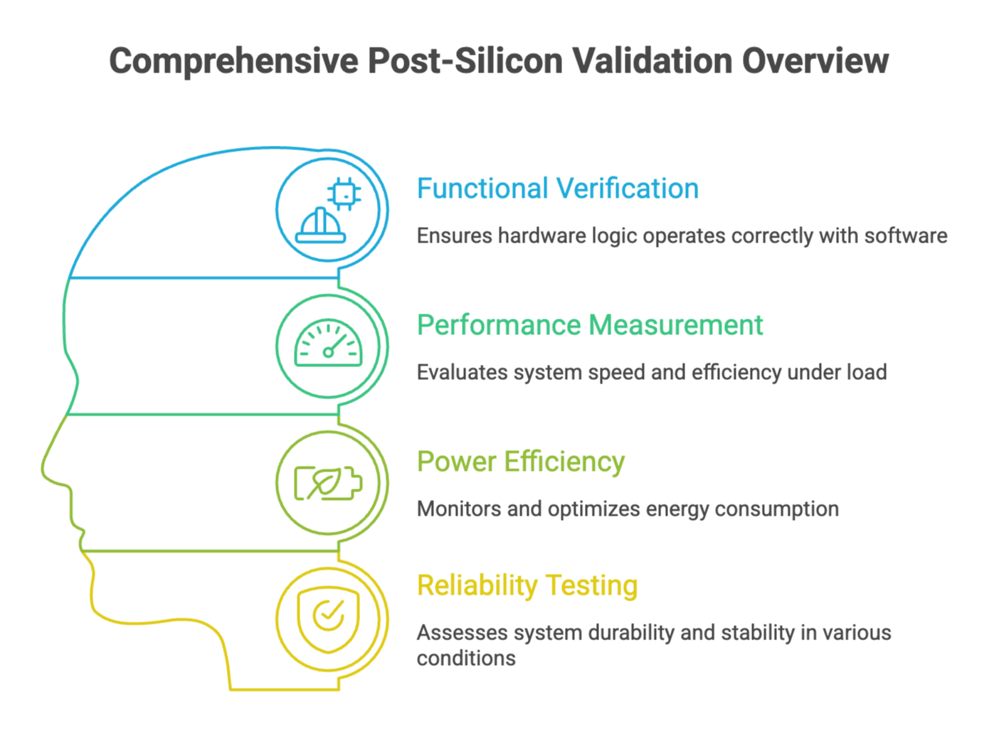
Unlike pre-silicon verification, which relies on simulation and emulation, post-silicon validation tests the actual hardware under real operating conditions. Engineers execute workloads, measure electrical behavior, analyze performance, identify defects, and verify interactions between different hardware blocks before the product enters mass production.
Because physical silicon often behaves differently from simulation models, post-silicon validation serves as the final safeguard against costly field failures. It also plays a vital role in improving overall semiconductor testing quality by identifying issues that may only appear after fabrication.
Why Post-Silicon Validation Is Becoming More Complex in the AI Era
As semiconductor devices continue to evolve, validating them has become significantly more challenging. Several technological advancements have increased both the scale and complexity of post-silicon validation.
Increasing SoC Complexity
Modern SoCs combine multiple processing cores, AI engines, memory controllers, security modules, high-speed interfaces, multimedia processors, and communication subsystems on a single chip.
Every subsystem must operate correctly on its own while also interacting seamlessly with every other component. Validating these interactions requires millions of test scenarios across different operating conditions.
As a result, comprehensive SoC Testing now involves significantly more engineering effort than in previous generations.
AI Accelerators Introduce New Validation Requirements
Dedicated AI hardware such as NPUs, tensor processors, and AI accelerators has introduced entirely new categories of validation challenges.
Engineers must verify:
- AI inference accuracy
- Data movement efficiency
- Accelerator scheduling
- Memory bandwidth utilization
- Quantization behavior
- Mixed-precision computation
- Power efficiency under AI workloads
Unlike traditional processors, AI engines process highly parallel workloads that generate unique traffic patterns throughout the chip, requiring specialized validation techniques.
Growing Number of High-Speed Interfaces
Today’s SoCs often integrate several high-speed communication standards, including:
- PCIe Gen6
- DDR5 and LPDDR5X
- USB4
- Ethernet
- MIPI
- UCIe
- CXL
Each interface must be validated independently while also ensuring reliable interoperability with other subsystems.
Even minor signal integrity or timing issues can cause intermittent failures that are extremely difficult to reproduce.
Advanced Packaging and Chiplet Integration
Modern semiconductor products increasingly rely on chiplets, 2.5D packaging, 3D ICs, and advanced heterogeneous integration.
Rather than validating a single monolithic die, engineers must evaluate communication between multiple interconnected dies, package substrates, memory stacks, and high-speed interconnects.
This significantly expands validation coverage and introduces new thermal, power, and signal integrity considerations.
Power Management Has Become More Dynamic
Modern SoCs frequently operate across multiple voltage domains and dynamically adjust frequency and voltage depending on workload requirements.
Validation teams must verify:
- Dynamic Voltage and Frequency Scaling (DVFS)
- Low-power modes
- Sleep state transitions
- Clock gating
- Power gating
- Thermal throttling
Testing these scenarios requires executing thousands of workload combinations under varying environmental conditions.
Software-Hardware Interaction Is More Critical Than Ever
Modern chips depend heavily on firmware, operating systems, device drivers, hypervisors, and application software.
Many functional issues appear only when software interacts with actual silicon.
Post-silicon validation therefore extends beyond hardware verification to include complete hardware-software integration testing across realistic operating environments.
Massive Validation Data Volumes
Every validation cycle generates enormous quantities of logs, trace data, waveform captures, telemetry, and performance metrics.
Manually analyzing this information has become increasingly impractical.
Engineering teams now rely on AI-assisted analytics to identify anomalies, prioritize failures, and accelerate root-cause analysis.
Shrinking Development Timelines
Semiconductor companies are expected to release increasingly sophisticated products within shorter market windows.
While chip complexity continues to increase, validation schedules continue shrinking.
Engineering teams must therefore improve automation while maintaining comprehensive validation coverage.
This growing demand has significantly increased the importance of advanced test engineering services capable of accelerating validation without compromising product quality.
Core Challenges in Testing Complex SoCs
Successfully validating today’s SoCs involves overcoming numerous technical challenges.
1. Functional Coverage
Ensuring every hardware block, interface, and operating mode has been adequately tested remains one of the largest validation challenges.
Hidden corner cases often appear only after millions of test iterations.
2. Debugging Intermittent Failures
Some defects occur only under specific workloads, voltage conditions, or thermal environments.
These intermittent failures are particularly difficult to reproduce and isolate.
3. Performance Validation
Engineers must confirm that fabricated silicon achieves its intended throughput, latency,
bandwidth, and computational performance across various workloads.
4. Thermal and Power Validation
High-performance AI workloads can create thermal hotspots and power fluctuations that influence long-term reliability.
Testing must therefore evaluate both electrical behavior and thermal characteristics simultaneously.
Strategies for Effective Post-Silicon Validation
Modern semiconductor teams are adopting smarter validation approaches to manage increasing complexity.
1. Build Validation Planning Early
Post-silicon validation should begin during the design phase rather than after fabrication.
Early planning allows engineers to define validation objectives, identify critical test scenarios, implement appropriate test hooks as part of DFT, prepare debug infrastructure, and reduce delays once silicon becomes available.
2. Prioritize Risk-Based Testing
Not every subsystem presents the same level of risk.
Engineering teams increasingly prioritize validation efforts around high-speed interfaces, AI accelerators, security modules, power management, and memory subsystems which are at higher risk of failures.
This approach improves resource utilization while accelerating overall chip testing activities.
3. Use Automated Validation Frameworks
Automation has become essential for validating modern SoCs.
Automated frameworks execute thousands of regression tests, collect performance metrics, monitor system health, and compare results without requiring continuous manual intervention.
Automation also improves repeatability and enables validation teams to focus on complex debugging instead of repetitive execution tasks.
Automating Post-Silicon Validation: Trends in High-Speed Debug and Traceability
4. AI-Driven Validation Strategies
Artificial intelligence is reshaping post-silicon validation by helping engineers analyze large datasets, identify hidden patterns, and reduce the time required to detect and resolve silicon issues.
Instead of manually reviewing millions of log entries and waveform captures, AI-powered tools can quickly highlight abnormal behavior and prioritize failures based on their impact. This allows validation teams to focus on resolving critical issues earlier in the validation phase.
5. Intelligent Failure Detection
Machine learning algorithms can compare validation results against expected behavior and automatically detect anomalies.
These systems help engineers:
- Identify unexpected hardware behavior
- Detect performance bottlenecks
- Recognize recurring failure patterns
- Prioritize high-risk issues
- Reduce manual debugging effort
This significantly accelerates semiconductor testing while improving validation accuracy.
6. Predictive Analytics
Historical validation data provides valuable insights for current and future projects.
AI models analyze previous failures, test coverage, and debug histories to predict which subsystems are more likely to experience issues. Engineers can then focus validation efforts on these high-risk areas, improving overall efficiency.
Advanced Debug Techniques for Complex SoCs
Debugging modern SoCs requires far more than traditional oscilloscopes and logic analyzers. Engineers rely on multiple hardware and software tools to isolate issues efficiently.
1. On-Chip Debug Features
Many advanced SoCs include built-in debug capabilities such as:
- Trace buffers
- Performance counters
- Embedded logic analyzers
- Hardware breakpoints
- Debug registers
These features provide real-time visibility into internal chip behavior without significantly affecting system performance.
2. FPGA Prototyping
FPGA prototypes allow engineers to validate software and hardware interactions before and after silicon becomes available.
Running real applications on FPGA platforms helps uncover integration issues early, reducing post-silicon debugging effort.
3. Emulation Platforms
Hardware emulators enable engineers to execute complex workloads much faster than simulation while providing deep visibility into system behavior.
Combined with post-silicon validation, emulation creates a more comprehensive testing strategy.
Best Practices for Successful Post-Silicon Validation
Successful validation depends on combining strong engineering processes with modern tools and methodologies.
Some widely adopted best practices include:
- Develop validation plans early in the project.
- Prioritize testing based on design risk.
- Automate repetitive validation workflows.
- Validate hardware and software together.
- Perform extensive stress and corner-case testing.
- Monitor power, thermal, and performance simultaneously.
- Use AI-assisted analytics for faster debugging.
- Continuously refine validation strategies using lessons learned from previous projects.
Following these practices helps reduce silicon re-spins while improving overall product reliability.
The Future of Post-Silicon Validation
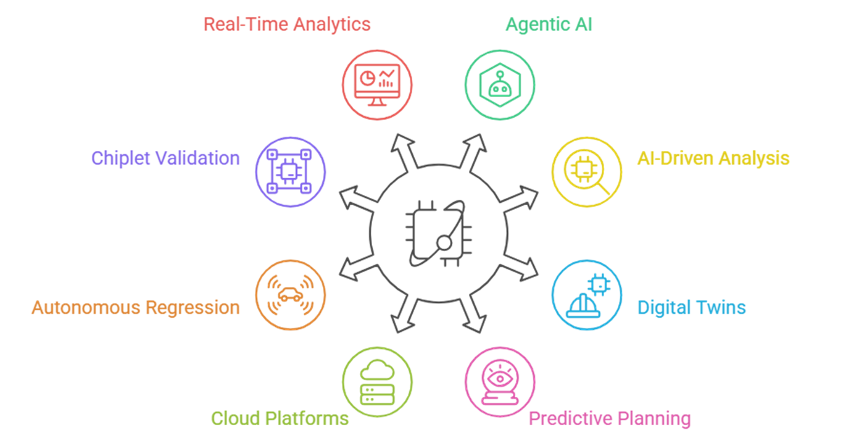
As semiconductor technology continues advancing, post-silicon validation will become increasingly intelligent, and data driven.
Several emerging technologies are expected to shape the future, including:
- Agentic AI for validation workflow orchestration
- AI-driven root-cause analysis
- Digital twins for silicon behavior modeling
- Cloud-based validation platforms
- Autonomous regression management
- Advanced chiplet validation techniques
- Real-time analytics for complex SoCs
Rather than replacing validation engineers, these technologies will enhance productivity by automating repetitive tasks and enabling faster engineering decisions.
As SoCs become more sophisticated, comprehensive SoC Testing and intelligent chip testing strategies will remain essential for delivering reliable, production-ready semiconductor devices.
Why Tessolve is Your Trusted Partner for Post-Silicon Validation
At Tessolve, we help customers validate complex semiconductor products using comprehensive engineering expertise spanning the complete silicon lifecycle.
- We provide post-silicon validation at component and system levels, silicon bring-up, characterization, qualification and reliability, failure analysis and complete product engineering services.
- Our capabilities cover ASICs, SoCs, chiplets, HPCs, Hyperscalars, GaN, SiC etc., ensuring reliable validation across modern designs.
- We combine deep semiconductor expertise with automation, advanced debug methodologies, and scalable validation workflows to improve test coverage and accelerate product readiness.
- Our integrated engineering approach helps customers reduce validation cycles, improve product quality, minimize silicon risks, and confidently transition designs from prototype to production.
Frequently Asked Questions
1. What is post-silicon validation in semiconductor development?
Post-silicon validation verifies fabricated chips under real operating conditions to ensure functionality, performance, reliability, and production readiness.
2. Why is post-silicon validation becoming more challenging?
Increasing SoC complexity, AI accelerators, advanced packaging, high-speed interfaces, and shorter development cycles make validation significantly more demanding.
3. How does AI improve post-silicon validation?
AI automates failure detection, analyzes validation data, predicts potential issues, and accelerates debugging through intelligent analytics and pattern recognition.
4. What are the main goals of SoC testing after fabrication?
The primary goals are verifying functionality, validating performance, identifying hardware defects, ensuring reliability, and preparing chips for mass production.
5. How does Tessolve support semiconductor validation and testing?
Tessolve provides end-to-end post-silicon validation, test engineering, characterization, failure analysis, DFT, and production test solutions for advanced semiconductor devices.