
Every time memory speeds jump, power and signal integrity take the hit. DDR5 and upcoming DDR6 interfaces push data rates so high and edge transitions so fast that subsystem design has become a tightrope walk. At the center of this headache is Simultaneous Switching Noise (SSN), better known as ground bounce, which continues to be a primary culprit behind memory errors.
Ground bounce occurs when multiple output drivers switch simultaneously, creating transient voltage fluctuations within the power distribution network. If not properly controlled, these fluctuations can introduce timing uncertainty, degrade signal integrity, and increase the likelihood of data errors. Addressing these challenges requires careful hardware design, robust power distribution planning, and optimized PCB implementation from the earliest stages of development.
What Is Simultaneous Switching Noise?
Simultaneous Switching Noise is an electrical phenomenon that occurs when multiple output signals change state at nearly the same time. As numerous drivers switch simultaneously, sudden changes in current flowing through shared power and ground paths generate unwanted voltage fluctuations.
These transient voltage variations appear across package inductance, PCB traces, vias, connectors, and other elements within the power distribution network. The resulting voltage disturbance is commonly referred to as ground bounce when it affects the ground reference or VDD droop when it impacts the power rail.
In high-speed DDR5 and DDR6 memory systems, where hundreds of signals may transition within extremely short intervals, even small voltage disturbances can influence signal quality and reduce overall system stability.
Why Does Ground Bounce Become More Critical In DDR5 and DDR6?
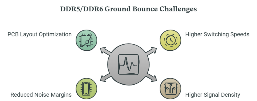
Signal integrity engineers have always had to watch out for ground bounce, but DDR5 and DDR6 take the difficulty to another level. With data rates climbing fast and voltage tolerances shrinking, even minor ground plane bounces can completely collapse timing windows and wreck noise margins.
Higher Switching Speeds
Modern memory interfaces operate at significantly higher transfer rates than previous generations. Faster signal transitions produce larger current spikes, increasing the impact of inductive effects throughout the power delivery network.
Higher Signal Density
Memory controllers and DIMMs now support more complex interfaces with larger numbers of simultaneously switching signals. As switching activity increases, cumulative current demand also rises, making SSN more difficult to control.
Reduced Noise Margins
As operating voltages continue to decrease, systems become increasingly sensitive to even small voltage disturbances. Ground bounce that may have been acceptable in earlier technologies can now consume a substantial portion of the available timing and voltage margin. These factors make SSN analysis an essential part of modern hardware design rather than a final-stage verification task.
Optimize PCB Layout
A well planned PCB board design plays an important role in reducing SSN. Designers typically focus on:
- Continuous ground reference planes
- Controlled impedance routing
- Shorter return current paths
- Reduced via transitions where practical
- Balanced layer stack-ups
- Proper spacing between critical signals
These practices contribute to improved signal integrity while reducing unwanted voltage fluctuations.
How to Manage Signal Integrity in High-Speed PCB Hardware Design
Why Is Simulation Important for SSN Analysis?
You won’t spot ground bounce during a quick schematic check; a clean diagram hides all the parasitic inductance and return path breaks. At today’s memory speeds, running pre- and post-layout SI/PI simulations is the only way to catch destructive rail noise before throwing money away on a dead board spin.
Signal integrity, power integrity, and electromagnetic simulations allow engineering teams to evaluate:
- Voltage ripple across power rails
- Ground bounce levels
- Return current behavior
- Crosstalk between signals
- Timing margins
- Power distribution performance
Finding and fixing signal integrity bugs early in the design cycle is always cheaper than troubleshooting prototype boards. Spotting these issues before sending files to the fab keeps your budget intact and prevents weeks of lost project time.
What Role Does PCB Engineering Play?
Modern PCB engineering extends well beyond component placement and routing. It involves optimizing the complete electrical behavior of the printed circuit board while balancing manufacturability, reliability, thermal performance, and signal integrity.
For DDR5 and DDR6 platforms, PCB engineering often includes:
- Layer stack-up optimization
- High-speed interface routing
- Power integrity planning
- Signal integrity analysis
- EMI-aware layout practices
- Design rule verification
- Manufacturing readiness checks
These engineering activities help improve overall system performance while supporting reliable operation under demanding workloads.
How Tessolve Supports Advanced Hardware Design
With DDR5 widely adopted and DDR6 on the horizon, managing simultaneous switching noise (SSN) has become increasingly important in advanced memory and high-speed hardware design. Tessolve helps engineering teams address SSN-related challenges through a combination of advanced PCB board design, signal integrity (SI), and power integrity (PI) expertise. Our engineers can support power-plane planning, stack-up optimization, high-speed routing, and SI/PI simulation to identify potential ground-bounce and signal-quality issues early in the design cycle.
Tessolve also brings hands-on lab validation into the process, helping teams correlate simulation results with real-world hardware behavior. This end-to-end approach enables engineering teams to identify risks earlier, optimize designs, and build reliable high-performance systems for next-generation memory applications.
Frequently Asked Questions
1. What is Simultaneous Switching Noise (SSN)?
Simultaneous Switching Noise occurs when multiple outputs switch simultaneously, creating transient voltage fluctuations that can affect signal integrity and power stability.
2. Why is ground bounce a concern in DDR5 and DDR6 systems?
Higher switching speeds, denser interfaces, and lower operating voltages make DDR5 and DDR6 memory systems more sensitive to voltage fluctuations caused by ground bounce.
3. How does PCB board design help reduce ground bounce?
You can’t eliminate SSN entirely, but a solid PCB board design stops it from wrecking your signals. Keeping power distribution impedance low and ensuring return currents have unbroken reference planes keeps voltage ripple under control when massive buses switch at once.
4. Why is PCB engineering important for high-speed memory interfaces?
Solid PCB engineering gives DDR5 and DDR6 designs the foundation they need to stay stable. Getting the stack-up right, controlling trace geometry on high-speed lines, and running early SI/PI simulations ensures your power rails stay quiet and your data transfers stay clean.
5. How does Tessolve support advanced hardware design?
Tessolve provides end-to-end hardware design, PCB engineering, simulation, mechanical engineering, manufacturing support, and validation services for complex electronic systems.