Modern electronic products are expected to process more data, operate at higher speeds, and deliver exceptional reliability. Whether it’s AI servers, automotive electronics, telecommunications equipment, industrial automation systems, or advanced consumer devices, high-speed hardware has become the foundation of innovation.
However, designing high-speed hardware is far more challenging than simply selecting faster processors or memory devices. As signal frequencies increase, engineers must carefully address signal integrity, power delivery, thermal management, electromagnetic interference (EMI), PCB layout, and manufacturability. A small design oversight can lead to performance degradation, system instability, or expensive redesigns.
In this blog, we’ll explore the key design considerations that help engineering teams build reliable, high-performance hardware for today’s demanding applications.
What is High-Speed Hardware Design?
High-speed hardware design involves developing electronic systems that reliably transmit and process high-frequency signals while maintaining performance, signal quality, and system stability.
Unlike conventional electronic products, high-speed systems require engineers to consider electrical behavior throughout the design process. Every trace, connector, via, and component placement can influence overall performance.
A successful hardware design balances electrical performance, thermal efficiency, manufacturability, and long-term reliability to ensure products operate consistently under demanding conditions.
Key Design Considerations for Building High-Speed Hardware
As data rates continue to increase, engineers must address several interconnected design challenges. Focusing on these considerations early helps reduce redesigns, improve product reliability, and accelerate development.
Signal Integrity
Signal integrity is one of the most critical aspects of high-speed hardware development. At higher frequencies, signals are more susceptible to distortion, reflections, crosstalk, and attenuation.
How to Manage Signal Integrity in High-Speed PCB Hardware Design
To maintain signal quality, engineers focus on:
- Controlled impedance routing
- Differential pair matching
- Trace length matching
- Proper termination techniques
- Minimizing discontinuities
These practices help ensure reliable communication between high-speed components.
PCB Stack-Up Planning
A well-designed PCB stack-up directly impacts signal integrity, power distribution, and electromagnetic performance.
Engineers carefully define:
- Layer arrangement
- Ground and power planes
- Dielectric materials
- Copper thickness
- Controlled impedance requirements
An optimized stack-up simplifies routing while improving overall electrical performance. This makes early planning essential for any professional PCB board design project.
Power Integrity
Stable power delivery is just as important as clean signal transmission.
High-speed processors, FPGAs, AI accelerators, and memory devices demand consistent voltage levels despite rapidly changing current loads.
Effective power integrity strategies include:
- Low-impedance power distribution networks
- Proper decoupling capacitor placement
- Optimized power planes
- Voltage noise reduction
- Current return path optimization
Strong power integrity improves system stability while minimizing unexpected failures.
Thermal Management
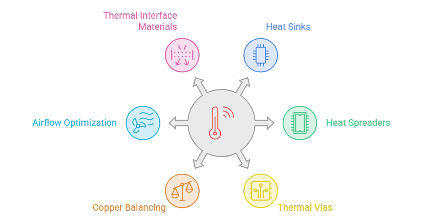
Higher processing speeds typically generate more heat.
Without proper cooling, excessive temperatures can reduce performance, shorten component lifespan, and impact overall system reliability.
Common thermal management techniques include:
- Heat sinks
- Heat spreaders
- Thermal vias
- Copper balancing
- Airflow optimization
- Thermal interface materials
Thermal analysis early in development helps prevent overheating before hardware reaches production.
Component Placement
Strategic component placement minimizes routing complexity while improving electrical performance.
High-speed components should be positioned to reduce signal path lengths and avoid unnecessary vias or sharp routing transitions.
Careful placement also improves power distribution, thermal performance, and manufacturing efficiency.
Routing Strategy
PCB routing becomes increasingly important as signal speeds rise.
Engineers must maintain consistent impedance, minimize skew, reduce crosstalk, and preserve signal quality throughout the routing process.
Important routing practices include:
- Short signal paths
- Differential pair routing
- Reference plane continuity
- Via optimization
- Proper spacing between traces
These techniques significantly improve communication reliability across high-speed interfaces.
Electromagnetic Compatibility (EMC) and EMI Control
High-frequency signals naturally generate electromagnetic emissions that can interfere with nearby circuits.
Reducing EMI requires careful attention to:
- Grounding strategies
- Shielding
- Return current paths
- Filter placement
- PCB layout optimization
Addressing EMC requirements early reduces compliance risks during product certification.
High-Speed Interface Support
Modern electronic products often integrate multiple high-speed interfaces operating simultaneously.
Examples include:
- PCIe
- USB4
- DDR5
- LPDDR5X
- Ethernet
- HDMI
- DisplayPort
- MIPI
Each interface introduces unique routing, timing, and signal integrity requirements that must be considered during the design phase.
Design for Manufacturability (DFM)
A technically sound design must also be practical to manufacture.
Design for Manufacturability ensures that PCB layouts can be fabricated, assembled, and tested efficiently without introducing unnecessary production costs or yield issues.
Early DFM reviews help identify manufacturing constraints before production begins, reducing costly revisions later.
Modern Technologies Improving High-Speed Hardware Development
Engineering teams increasingly rely on advanced technologies to simplify complex hardware development.
Some of the most impactful include:
- AI-assisted PCB layout optimization
- Predictive signal integrity analysis
- Digital twins for hardware validation
- 3D electromagnetic simulation
- Automated Design Rule Checking (DRC)
- Concurrent ECAD-MCAD collaboration
- Advanced thermal simulation
These technologies improve design accuracy while reducing development time and engineering effort.
Organizations offering professional PCB design service solutions increasingly integrate AI-driven analysis and simulation into modern hardware development workflows.
Why Tessolve is Your Trusted Partner for High-Speed Hardware Development
At Tessolve, we help customers transform complex hardware concepts into production-ready products through comprehensive engineering expertise.
- We provide PCB design, high-speed board design, embedded hardware development, system board design, PCB manufacturing support, validation, verification, and complete product engineering services.
- Our expertise spans high-speed digital hardware, signal integrity, power integrity, thermal analysis, and complex multi-layer PCB board design for demanding applications.
- We support industries including automotive, industrial automation, communications, consumer electronics, healthcare, and semiconductor markets with scalable engineering solutions.
- Our integrated engineering approach helps customers improve design quality, accelerate product development, and efficiently bring reliable, high-performance hardware to market.
Frequently Asked Questions
1. What is high-speed hardware design?
High-speed hardware design focuses on developing reliable electronic systems that support fast data transmission while maintaining signal integrity and performance.
2. Why is signal integrity important in high-speed hardware?
Good signal integrity prevents data errors, reflections, crosstalk, and interference, ensuring stable communication between high-speed electronic components.
3. How does PCB stack-up affect hardware performance?
A well-planned PCB stack-up improves signal integrity, power distribution, electromagnetic compatibility, and overall system reliability in high-speed designs.
4. What challenges are common in high-speed PCB design?
Common challenges include routing complexity, power integrity, thermal management, EMI control, controlled impedance, and meeting manufacturability requirements.
5. How does Tessolve support high-speed hardware development?
Tessolve provides PCB design, embedded hardware development, validation, verification, and product engineering for advanced high-speed electronic systems.