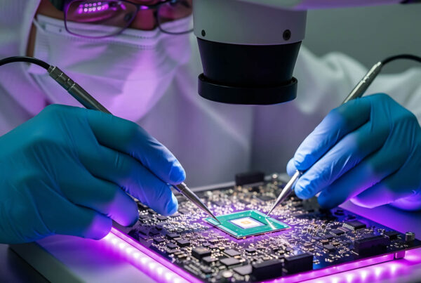
We live in an age where technology is becoming the steering wheel of evolution. A printed Circuit Board (PCB) is one such component that is indispensable in modern life. For instance, the PCB is a foundation for many internal computer components, such as video cards, network interface cards, etc. Furthermore, it is also used in almost every electrical and electronic component.
Over time, technological advancements are taking place in PCB design, like making circuit boards smaller, higher-speed, and more flexible. However, these gains come with significant challenges, and Signal Integrity (SI) is at the forefront. With data rates now pushing 224 Gbps per lane, even the smallest physical discontinuity can render a multi-million dollar system inoperable.
Understanding the High-Speed PCB Design and Signal Integrity
High-speed PCB design refers to designing PCBs for electronic systems that require data transmission at Higher speeds. typically, where the signal’s rise time is less than the propagation delay of the trace. It aids in various industries, including data communication, telecommunication, radar systems, etc. Designing such PCBs demands expertise; hence, PCB hardware design services become crucial.
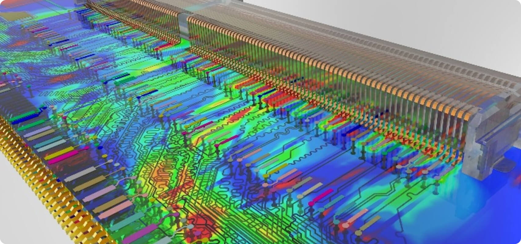
Maintaining Signal Integrity (SI) is paramount in high-speed PCB design. Signal integrity issues, such as reflections, crosstalk, and impedance mismatches, can degrade signal quality, leading to data errors and communication failures.Nowadays, “Loss Budgets” have become so tight that designers must account for the “glass weave effect” (skew caused by the physical fiberglass pattern) and advanced PAM4/PAM16 signaling levels, which reduce noise margins significantly.
As signal frequencies increase, the wavelength of signals becomes comparable to the physical dimensions of the PCB traces, making it challenging to control impedance and prevent signal distortions.
Challenges Associated With High-Speed PCB Design
- Electromagnetic Interference (EMI)
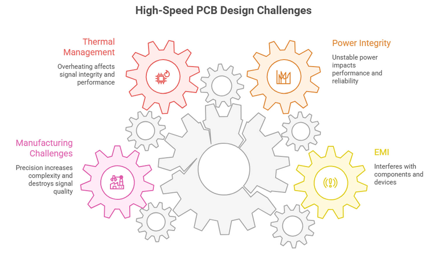
High-speed signals generate electromagnetic fields that can interfere with other components on the PCB and nearby electronic devices. EMI can lead to increased noise levels, affecting the system’s overall performance and potentially violating regulatory requirements. Mitigating EMI requires the implementation of shielding, proper grounding techniques, and the use of low-impedance power distribution networks.Designers should also consider the placement of components and the routing of high-speed traces to minimize loop areas, which can act as antennas and radiate electromagnetic energy. Designers are increasingly using “Faraday cages” embedded directly within the PCB layers for extreme isolation. Additionally, the use of ferrite beads, filters, and other EMI suppression components can be employed to reduce electromagnetic emissions.
- Power Integrity
High-speed designs often require careful consideration of power distribution to ensure that all components receive stable and noise-free power. Power integrity issues, such as voltage drops, ground bounce, and power plane resonances, can impact the performance and reliability of the PCB. As modern CPUs and GPUs now demand hundreds of Amps at sub-1.0V levels, a voltage drop of even 50mV can cause a complete system failure.To address power integrity challenges, designers should optimize power plane designs, minimize loop inductance, and use decoupling capacitors strategically. Advanced power integrity analysis tools can simulate and predict the behavior of power distribution networks, aiding in the identification and resolution of potential issues.
- Thermal Management
High-speed electronic components generate significant heat, and effective thermal management is crucial to prevent overheating and ensure reliable operation. Thermal issues can arise due to high power densities, inadequate heat dissipation, or poor component placement. Thermal gradients can lead to changes in material properties, affecting signal integrity and overall system performance.Designers must carefully select materials with appropriate thermal conductivity, use heat sinks and thermal vias to dissipate heat, and optimize the layout to facilitate efficient thermal transfer. Thermal simulation tools can help predict and address potential thermal issues during the design phase.
- Manufacturing Challenges
Fabricating high-speed PCBs poses unique manufacturing challenges. The precision required for tight tolerances, controlled impedance, and fine-pitch components increases the complexity of the manufacturing process. At data rates of 224 Gbps, even a standard “via stub” (unused hole depth) acts as an antenna, destroying signal quality. Techniques like “Back-drilling” and “Microvias” are now mandatory to maintain performance.Collaboration between design and manufacturing teams is essential to arrive at a balanced stackup that meets both Signal performance and Manufacturability requirements. Design for Manufacturability (DFM) guidelines should be followed, and prototypes should be.
Understanding the Difference: Hardware Design vs. PCB Design
Choose Tessolve
High-speed PCB design presents a myriad of challenges that require careful consideration and expertise. Tessolve is a renowned platform that provides turnkey PCB design and manufacturing. We use AI-assisted routing and predictive SI/PI analysis to evaluate thousands of placement strategies, ensuring optimal performance for 800G Ethernet, PCIe Gen 6/7, and AI acceleration boards.
We provide high-end production and assembly services through partner and client-qualified PCB Fabs, EMS, and CM companies. We possess a team of designers who have gone through extensive training. Moreover, we have partnered with major EDA companies and offer a holistic range of tools to support any customer with top-notch hardware design.
Let’s Transform Possibilities Into Next-gen Products
Frequently Asked Questions
1. What are the common challenges in implementing high-speed signal interfaces in vehicles?
Automotive designers face extreme temperatures, humidity, and electromagnetic interference while maintaining data rates above 10 Gbps for ADAS.
2. How do signal integrity tools impact high-speed interface development?
These tools identify crosstalk and reflections early, reducing costly physical prototypes and ensuring first-pass compliance with 2026 standards.
3. What solutions exist for system and board-level signal integrity analysis?
Advanced EDA simulators like Sigrity X and hardware tools like high-bandwidth oscilloscopes enable precise time-domain and S-parameter modeling.
4. What tools support high-speed PCB design for next-gen electronics?
Enterprise platforms like Allegro X and Altium Designer 2026 offer AI-assisted routing, unified database management, and integrated thermal-aware simulation.