

At 3nm, success isn’t just about innovation; it’s about precision. The margin for error has shrunk so dramatically that even a minor oversight in sign-off can lead to costly re-spins, delays, or performance failures. For modern chip design, sign-off has evolved from a final checkpoint into a continuous, integrated discipline that begins early and runs throughout the design lifecycle.
If you’re aiming for first-pass tape-out success, you need more than good engineering; you need the right strategies, tools, and mindset. Let’s explore what it really takes.
Why 3nm Sign-off is a Different Game
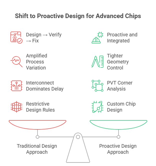
At advanced nodes like 3nm, complexity doesn’t just increase; it explodes. Designs now involve billions of transistors, tighter geometries, and extreme variability.
What makes sign-off particularly challenging?
- Process variation is amplified: Tiny manufacturing differences can significantly impact performance.
- Interconnect dominates delay: Wires, not transistors, are now the primary bottleneck.
- More PVT corners to analyze: Hundreds of scenarios must be validated simultaneously.
- Design rules are extremely restrictive: EUV and multi-patterning constraints limit flexibility.
In this environment, traditional “design → verify → fix” approaches no longer work. Instead, sign-off must be proactive and tightly integrated into custom chip design workflows.
Core Sign-off Strategies for Achieving First-Pass 3nm Tape-out
1. Shift-Left Sign-off Methodology
One of the most effective strategies is adopting a shift-left approach, bringing sign-off checks earlier into the flow.
Instead of waiting until the end:
- Run early DRC/LVS checks during placement and routing
- Integrate timing and power analysis during floor planning
- Continuously validate manufacturability constraints
This reduces late-stage surprises and shortens iteration cycles. Historically, relying on post-design verification created bottlenecks, but integrating sign-off during implementation significantly improves closure timelines.
For chip design companies, this approach is now essential to meet aggressive tape-out schedules.
2. Master MCMM (Multi-Corner Multi-Mode) Closure
At 3nm, MCMM analysis is not optional; it’s foundational.
Designs must meet timing across:
- Multiple voltages
- Temperature variations
- Process corners
- Functional modes
The challenge? You could be dealing with hundreds of scenarios simultaneously.
Best practices include:
- Prioritizing critical paths instead of treating all equally
- Using unified timing graphs for concurrent optimization
- Automating scenario pruning to reduce runtime
Without strong MCMM strategies, timing closure becomes nearly impossible, and missed timing is one of the top reasons for tape-out failure.
3. Sign-off-Aware Physical Design
At 3nm, physical design decisions directly impact sign-off success.
Key focus areas:
a) Congestion and Routing
Routing congestion can introduce crosstalk, noise, and timing violations. Dense routing pitches make signal integrity a major concern.
Strategy:
- Perform early congestion analysis
- Use layer-aware routing
- Optimize floor plans before detailed routing
b) RC Parasitics Management
RC delay dominates timing budgets at advanced nodes.
Strategy:
- Accurate parasitic extraction
- Strategic buffering and shielding
- Use higher metal layers for long routes
c) Power Integrity
IR drop and voltage fluctuations can create unpredictable delays.
Strategy:
- Design robust power delivery networks (PDN)
- Use advanced techniques like backside power delivery
All these factors must be validated continuously, not just at final sign-off.
4. Advanced Timing Closure Techniques
Timing closure at 3nm is no longer just an engineering step; it’s a competitive differentiator.
To achieve first-pass success:
- Use statistical timing models (AOCV/POCV) to capture variation
- Apply timing-driven placement and routing
- Optimize clock tree synthesis (CTS) for skew and latency
- Balance setup and hold violations carefully
Also, remember:
- Every picosecond matters at 3nm
Even small inefficiencies can push designs out of spec, especially in high-performance applications like AI chips.
5. Reliability and Manufacturability Sign-off
At 3nm, passing timing isn’t enough; you must ensure long-term reliability.
Key checks include:
- Electromigration (EM): High current density can damage interconnects
- Thermal analysis: Heat buildup affects performance and lifespan
- Signal integrity: Crosstalk and noise must be minimized
Electromigration and thermal issues are significantly worse at smaller nodes due to higher current densities and compact layouts.
Ignoring these can result in chips that pass initial tests but fail in the field, a costly mistake for any custom chip design project.
6. Leverage AI and Automation
Manual optimization is no longer scalable at 3nm.
Modern flows increasingly rely on:
- AI-driven ECO (Engineering Change Orders)
- Machine learning for congestion prediction
- Automated timing optimization engines
AI is rapidly becoming a necessity, not a luxury, especially for leading chip design companies working on complex SoCs.
7. Tight Correlation Between Tools and Sign-off
One of the biggest risks in advanced node design is tool mismatch.
If implementation tools and sign-off tools are not well correlated:
- Timing differences can emerge late
- DRC violations may reappear
- Multiple ECO loops may be required
Best practices:
- Use sign-off-aware implementation tools
- Ensure consistent extraction models
- Validate correlation early and often
The goal is simple:
What you see during implementation should match the final sign-off results.
8. Continuous Verification Mindset
Gone are the days of sequential flows.
At 3nm, successful teams:
- Run parallel verification flows
- Continuously validate timing, power, and physical constraints
- Iterate rapidly with smaller ECO cycles
This concurrent approach reduces last-minute surprises and ensures smoother tape-out readiness.
How Tessolve Enables First-Pass 3nm Tape-out Success
At Tessolve, we understand that achieving first-pass tape-out at 3nm demands more than just tools; it requires deep domain expertise, proven methodologies, and a highly integrated approach.
We bring decades of experience in advanced-node chip design, helping global clients navigate the complexities of 3nm and beyond. Our end-to-end capabilities span physical design, timing closure, sign-off verification, and silicon validation, ensuring every aspect of your design is optimized for manufacturability and performance.
Our teams leverage sign-off-aware flows, AI-driven optimization techniques, and robust MCMM strategies to accelerate convergence while minimizing risk. Whether it’s handling RC challenges, power integrity, or reliability checks, we deliver precision at every stage.
For organizations seeking reliable partners in custom chip design, Tessolve stands out among leading chip design companies by consistently enabling faster, first-pass silicon success.
Frequently Asked Questions
1. Why is sign-off more challenging at 3nm compared to older nodes?
At 3nm, tighter geometries, higher variability, and complex rules make timing, power, and reliability closure significantly harder.
2. What is first-pass tape-out success, and why is it important?
It means achieving a functional chip without re-spins, saving time, reducing costs, and accelerating product time-to-market.
3. How does shift-left methodology improve sign-off outcomes?
It catches issues earlier in the design cycle, reducing late-stage fixes, minimizing iterations, and improving overall tape-out success rates.
4. What role does MCMM analysis play in 3nm designs?
MCMM ensures timing closure across multiple scenarios like voltage, temperature, and modes, preventing failures under real-world operating conditions.
5. Can AI really help in chip sign-off at advanced nodes?
Yes, AI accelerates optimization, predicts issues early, reduces manual effort, and improves correlation between design and final sign-off results.