
Realize next-gen chips and systems – on robust engineering
Your Semiconductor Engineering Partner
As a semiconductor design company, Tessolve provides end-to-end engineering expertise across chip design, verification, validation, testing, and product engineering. We help semiconductor companies navigate complex development challenges and move from design intent to production-ready silicon.
With deep experience across digital, analog, mixed-signal, and SoC development, our semiconductor engineering services support customers across the product lifecycle, helping accelerate development while maintaining performance, quality, and reliability.
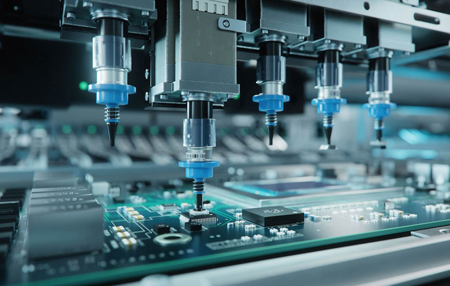
Innovating Possibilities To Products
An extended arm of semiconductor firms
Semiconductors are getting compact by the day. Developing them is getting complex. We’re simplifying complexities while catalyzing the productization of System-on-Chip, supporting faster GTMs without loss of performance and integrity. Almost two decades of engineering expertise empower us with knowledge, and make us a contender for the title of the best semiconductor company. We’re straightforward in what works and what wouldn’t – driving ideas to the final product actively.
Engineering Solutions
End-to-end – VLSI to Hardware for a first-pass product
Custom Silicon
We provide complete custom silicon development, covering architecture, design, integration, and validation. With a focus on advanced technologies like the 3nm process node, Heterogeneous Integration, AI/ML Accelerator design, and UCIe (Chiplet) architectures. Our engineering teams work closely with customers to shape solutions tailored to their product needs. We focus on predictable execution and high-quality delivery at every stage. We also ensure robust Security and Functional Safety, supporting requirements like Hardware Root of Trust (HRoT) and ISO 26262 compliance. With strong technical support and clear communication, we ensure a smooth development journey.Pre Silicon Design
We provide complete custom silicon development, covering architecture, design, integration, and validation. With a focus on advanced technologies like the 3nm process node, Heterogeneous Integration, AI/ML Accelerator design, and UCIe (Chiplet) architectures. Our engineering teams work closely with customers to shape solutions tailored to their product needs. We focus on predictable execution and high-quality delivery at every stage. We also ensure robust Security and Functional Safety, supporting requirements like Hardware Root of Trust (HRoT) and ISO 26262 compliance. With strong technical support and clear communication, we ensure a smooth development journey.I am raw html block.
Click edit button to change this html
Post Silicon
Our focus is on the developed hardware and supporting software testing and verification, leveraging a proven validation approach, besides pre-silicon characterization and qualification competencies. This includes a specialized Validation Focus for HPC/AI accelerators and deep expertise in System-Level Test (SLT) for high-demand systems. The outcome is a first-pass product with near-zero defects within a lesser time frame than semiconductor engineering.Hardware Design and Turnkey Manufacturing
Hardware is a critical piece of Chip and Systems development. We address this with 200+ PCB Designers who can design and develop ATE boards, System boards, and Reliability and Evaluation boards, achieving a remarkable 99% First Pass Success Rate. Our domain expertise includes RF, mixed-signal, Digital, and analogue boards. We have built the necessary infrastructure required to optimize our HW designs, including library development, BOM management, and simulations.Chip Design
Our <a href=”/chip-design/”>VLSI design</a> team provides customers with semiconductor engineering solutions from RTL to GDS II. With our digital and analogue expertise combined, we are uniquely positioned to address a variety of chips at advanced process nodes. We know how to take your chip to market by providing strategy along with implementation. We can integrate into your existing team or become an extension of your process. As a value-add, our deep semiconductor testing expertise allows us to plan a DFT strategy that ensures faster silicon bring-up.
Package Engineering
Chip design is only a job half done. We realize in our semiconductor design services that the actual product depends on in-depth packaging and fabrication expertise, using the latest in semiconductor materials technologies at a competitive price point. From the right wafers to the underfill – we leverage the best resources to deliver advanced packaging semiconductor integrations.
<h3><strong>Post Silicon</strong></h3>
Focus on the developed hardware and supporting software testing, like system-level testing semiconductor and verification, leveraging a proven validation approach besides pre-silicon characterization and qualification competencies. The outcome is a first-pass product with near zero defects within a lesser time frame of semiconductor engineering.
<h3><strong>Hardware Design & Manufacturing</strong></h3>
Hardware is a critical piece of Chip and Systems development. We as a semiconductor services company address this with 200 <a href=”/hardware-design/”>PCB designers</a> who can design and develop ATE boards, System boards, and Reliability and Evaluation boards. Our domain expertise includes RF, Mixed Signal, Digital, and Analog boards. We have built the necessary infrastructure required to optimize our HW designs including library development, BOM management, and simulations.
<h3><strong>Industries</strong></h3>
Continuous investment of technical expertise has enabled us to handhold customers right from the specification stage through the entire product life cycle. Keeping pace with the increasing complexity and rising demands in the semiconductor space, such as semiconductor testing and advanced packaging semiconductor, we have evolved beyond our role as an engineering services provider.
Expertise In A Nutshell
Mastery of diverse signals and ATE platforms

End-to-end semiconductor solution development – from chip design, test, and PCB engineering through post-silicon support.

Faster time-to-market through deep domain expertise in Analog, Digital, Mixed Signal, and RF.

Broad ATE platform experience and built-in infrastructure including a test floor, characterization, reliability lab, and PCB FAB.

The ability for clients to leverage high-end semiconductor engineering in a cost-effective model as we scale teams to meet the exact customer needs.
Expertise To Outcomes
Leading good ideas to great products
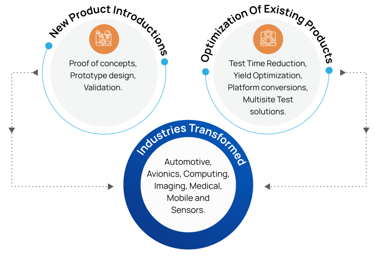
Expertise In A Nutshell
Mastery of diverse signals and ATE platforms
End-to-end semiconductor solution development – from chip design, test, and PCB engineering through post-silicon support.
Faster time-to-market through deep domain expertise in Analog, Digital, Mixed Signal, and RF.
Broad ATE platform experience and built-in infrastructure including a test floor, characterization, reliability lab, and PCB FAB.
The ability for clients to leverage high-end semiconductor engineering in a cost-effective model as we scale teams to meet the exact customer needs.
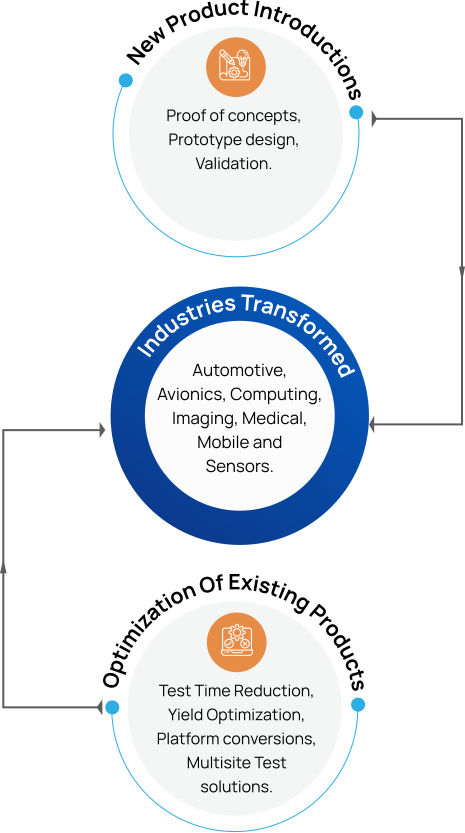
Expertise To Outcomes
Leading good ideas to great products
Advanced System Integration (Chiplets)
We offer the capability to design, architect, and manage complex systems composed of multiple specialized dies, known as Chiplets. This approach allows for unprecedented flexibility, performance scaling, and cost efficiency in semiconductor solutions. Our expertise covers the full spectrum of Chiplet integration, including physical layer design, inter-die communication, and validation. We actively work with industry standards critical for next-generation systems, such as UCIe (Universal Chiplet Interconnect Express), CXL (Compute Express Link), and HBM (High Bandwidth Memory) integration. This commitment to future-forward technology solidifies our position as the best semiconductor company for complex integration challenges.
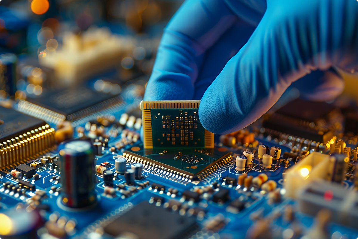

Experience Tessolve’s Innovating Engineering Excellence
A leading semiconductor company in the USA, Tessolve is dedicated to pushing the boundaries of innovation. With a commitment to engineering excellence, we deliver cutting-edge solutions across diverse sectors. Our customer-centric approach ensures tailored solutions that exceed expectations, fostering long-lasting partnerships globally.
Join us on the journey to unlock the full potential of technology with Tessolve.
FAQs
1. What are semiconductor solutions?
Semiconductor solutions cover the engineering activities involved in developing and bringing semiconductor products to market, including chip design, verification, DFT, physical design, silicon validation, testing, and product engineering.
2. What are the key stages in semiconductor product development?
The semiconductor development lifecycle typically spans architecture and design, verification, physical implementation, tape-out, silicon bring-up and validation, characterization, testing, and production support.
3. What is the difference between semiconductor design and semiconductor engineering?
Semiconductor design focuses on creating the chip architecture, circuitry, logic, and physical implementation. Semiconductor engineering extends beyond design into verification, silicon validation, test engineering, characterization, and product-level support.
4. Why is semiconductor testing important?
Semiconductor testing identifies manufacturing and functional defects, validates device performance, and supports yield and reliability improvements. It typically includes test development, characterization, production testing, and failure analysis.
5. What semiconductor engineering services does Tessolve provide?
Tessolve provides end-to-end semiconductor engineering services spanning chip architecture, digital, analog and mixed-signal design, verification, DFT, physical design, silicon validation, test engineering, and product engineering.
6. Is Tessolve a semiconductor design company?
Yes. Tessolve is a semiconductor design and engineering company with Spec-to-GDSII capabilities across digital, analog, and mixed-signal designs, complemented by post-silicon validation and test engineering.
7. What makes Tessolve’s semiconductor solutions different?
Tessolve brings semiconductor design, validation, and test engineering capabilities together across the product lifecycle. This combination provides continuity from design and verification through silicon validation, characterization, and testing.
8. Which semiconductor process technologies does Tessolve support?
Tessolve has semiconductor design experience spanning 2nm to 350nm process technologies, supporting advanced and mature technology requirements across digital, analog, and mixed-signal designs.