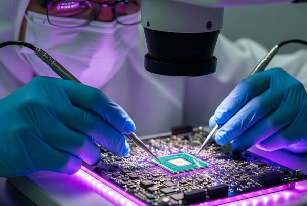
The domain of electronics is in a constant state of evolution, driven by technological advancements that continually push the limits of miniaturization, performance, and efficiency. At the bottom of these progressions lies the Printed Circuit Board (PCB), which forms the intricate network of connections vital for bringing electronic components to life. Historically, PCB design has been a meticulous process heavily reliant on the expertise and experience of human designers. Nevertheless, the recent surge of Artificial Intelligence (AI) is reshaping this field, ushering in a new era of automation and optimization in PCB design. AI is no longer just a plugin; it is the core engine that enables designers to tackle 800G networking and advanced AI accelerator boards with over 28 layers.
Challenges in Traditional PCB Design
While traditional design methods have served us well, they come with inherent limitations. Manually laying out complex circuits can be time-consuming and prone to errors. Traditional rule-based DRCs (Design Rule Checks) often fail to capture the multi-physics interactions between high-speed signals and thermal hotspots. Keeping pace with the ever-increasing density of modern electronics can be a constant struggle for design teams.
Get in touch
AI Guides in a New Era of Efficiency
AI Guides in a New Era of Efficiency
AI offers a powerful solution to these challenges. By leveraging machine learning algorithms and vast datasets of existing designs, AI tools can automate many of the tedious and error-prone tasks involved in PCB design. This translates to several key benefits:
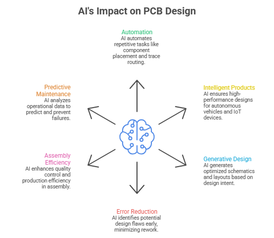
- Automation of Repetitive Tasks: AI algorithms now automate component placement and trace routing by considering thousands of permutations in minutes. Reinforcement learning agents can now solve complex BGA breakouts and differential pair symmetry with a first-pass yield of over 95%.
- Intelligent Products and Applications: The rise of autonomous vehicles and 6G-ready IoT devices demands high-performance PCB designs. AI-driven tools ensure these boards meet strict EMI/EMC compliance before a single prototype is built.
- Generative Design Optimization: Generative AI for hardware now allows engineers to define “design intent” (e.g., “Connect MCU to Display with 50-ohm impedance”) and let the software generate optimized schematics and layouts. This leads to smaller board sizes and improved thermal management.
- Reduced Errors: AI-powered tools can identify potential design flaws early in the process, minimizing the need for costly rework and delays.
- PCB Assembly and Manufacturing: The use of AI in PCB assembly and manufacturing processes is growing. Artificial intelligence (AI) can identify flaws and faults on PCBs using visual recognition algorithms, enhancing quality control. AI algorithms can also improve PCB designing and assembly procedures, increasing production and assembly efficiency.
- Fault Diagnosis and Predictive Maintenance: AI makes fault diagnosis and predictive maintenance possible by examining operational data from PCB systems. Artificial Intelligence (AI) can identify possible abnormalities and failures by analyzing sensor data and other pertinent characteristics. This allows for proactive maintenance, which lowers repair costs and downtime.
AI in Action: Automation and Optimization Techniques
Several AI-powered techniques are transforming the PCB design landscape:
- Automated Component Placement: AI algorithms can analyze factors like signal length, heat dissipation, and manufacturability to suggest optimal placement for each component on the PCB. This eliminates the need for manual trial-and-error approaches, saving designers valuable time and effort.
- Intelligent Routing: AI analyzes electrical characteristics and suggests routing paths that minimize signal loss. For high-speed interfaces like PCIe Gen 6 and HBM3, AI ensures signal latency is reduced by up to 20% by minimizing trace lengths and via counts.
- Thermal Analysis and Management: AI algorithms can predict heat distribution across the PCB based on component power consumption. This allows designers to identify potential overheating issues and implement effective cooling strategies.
- Design Rule Checking (DRC) and Electrical Rule Checking (ERC): In 2026, AI-enhanced DRCs are context-aware, reducing false positives and prioritizing violations that affect high-speed performance or manufacturing yield.
- Predictive Maintenance for Manufacturing: By analyzing historical data and identifying patterns in component failures, AI can predict potential issues during manufacturing. This allows for preventative maintenance and reduces the risk of production delays.
Benefits for PCB Design Services and Hardware Design Companies
The integration of AI into PCB design services presents several advantages for design companies:
- Faster Time-to-Market: With AI-powered tools accelerating the design process, companies can bring products to market quicker, gaining a competitive edge.
- Reduced Design Costs: Automation and optimization techniques can lead PCB hardware design organizations to significant cost savings by minimizing rework, optimizing material usage, and reducing development time.
- Enhanced Design Quality: AI-powered tools help ensure designs meet stringent quality standards, leading to more reliable and robust products.
- Improved Design Expertise: AI can act as a valuable assistant to designers, augmenting their expertise and allowing them to focus on more complex design challenges.
- Augmented Expertise: AI acts as a “Senior Electrical Engineer” assistant, handling complex routing while human designers focus on high-level architecture and creative problem-solving.
The Future of PCB Design: A Collaborative Approach
While AI offers tremendous potential for designing PCBs, it’s important to remember that it’s not meant to replace human designers entirely. The ideal scenario is a collaborative approach where AI handles repetitive tasks and automates optimization processes while human designers leverage their expertise for critical decision-making and creative problem-solving.
As AI technology continues to evolve, we can expect even more sophisticated tools and techniques to emerge. The future of PCB design promises to be a fascinating one, characterized by increased efficiency, unparalleled optimization, and a seamless collaboration between human ingenuity and the power of AI.
Download Brochure
Hardware Brochure
Tessolve provides turnkey PCB solutions from schematic design to layout to thoroughly tested assembly
Case Study PDF Download
Let’s Sum Up
The future of PCB design is undeniably intertwined with the power of AI. At Tessolve, we are at the forefront of this revolution, leveraging cutting-edge AI tools and techniques alongside our team of seasoned design experts. We offer a comprehensive suite of PCB design services, from initial concept to production, ensuring the highest quality, efficiency, and reliability for your project. Whether you require complex high-density interconnect (HDI) boards or cutting-edge mixed-signal designs, Tessolve’s AI-powered design approach can deliver optimal results. Contact us today and experience the future of PCB design.
Frequently Asked Questions
1. What are the leading features in modern PCB design automation?
2026 tools feature generative AI layout, real-time thermal-aware placement, and autonomous multi-agent systems for signal integrity sign-off.
2. What is the role of AI in PCB layout optimization?
AI acts as a co-pilot, reducing trace lengths by 28%, optimizing heat gradients, and accelerating prototyping cycles through predictive learning.
3. What are the current optimization techniques in electronic design?
Key techniques include reinforcement learning for auto-routing, 3D thermal simulation, and genetic algorithms for high-speed component placement and spacing.
4. How can designers leverage AI to reduce errors in PCB layout?
Designers use agentic AI to predict manufacturability scores (95%+ accuracy) and flag signal integrity risks before physical board fabrication.
5. How does AI-powered constraint management impact signal and power integrity?
AI dynamically adjusts trace widths and spacing, reducing crosstalk by 32% and signal reflections by 26% through deep-learning analysis.